
User manual

14-PIN SOIC/DIP/TSSOP
EVALUATION BOARD USER’S GUIDE
© 2006 Microchip Technology Inc. DS51597A-page 17
Appendix A. Schematic and Layouts
A.1 INTRODUCTION
This appendix contains the schematics and layouts for the 14-Pin SOIC/DIP/TSSOP
Evaluation Board. Diagrams included in this appendix:
• Board Schematic - Digital Circuitry
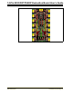
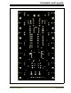
• Board – Top Layer + Bottom Layer + Silk-Screen
• Board – Top Layer + Silk-Screen
• Board – Bottom Layer
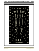
• Board – Power Plane
• Board – Ground Plane
• Board – Component Layer
A.2 SCHEMATICS AND PCB LAYOUT
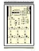
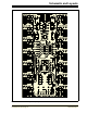
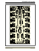
Figure A-4 shows the schematic of the 14-Pin SOIC/DIP/TSSOP Evaluation Board.
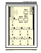
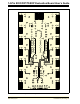
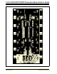
Figure A-2 shows the layout for the top layer of the 14-Pin SOIC/DIP/TSSOP
Evaluation Board. The layer order is shown in Figure A-1.
FIGURE A-1: Layer Order.
Top Layer
Ground Layer
Power Layer
Bottom Layer