SC70-6 and SOT23-6/8 to DIP-8 Evaluation Board User’s Guide © 2009 Microchip Technology Inc.
Note the following details of the code protection feature on Microchip devices: • Microchip products meet the specification contained in their particular Microchip Data Sheet. • Microchip believes that its family of products is one of the most secure families of its kind on the market today, when used in the intended manner and under normal conditions. • There are dishonest and possibly illegal methods used to breach the code protection feature.
SC70-6 AND SOT-23-6/8 TO DIP-8 EVALUATION BOARD USER’S GUIDE Table of Contents Preface ........................................................................................................................... 5 Chapter 1. Product Overview 1.1 Introduction ..................................................................................................... 9 1.2 What is the SC70-6 and SOT-23-6/8 to DIP-8 Evaluation Board? ................. 9 1.
SC70-6 and SOT-23-6/8 to DIP-8 Evaluation Board User’s Guide NOTES: DS51874A-page 4 © 2009 Microchip Technology Inc.
SC70-6 AND SOT-23-6/8 TO DIP-8 EVALUATION BOARD USER’S GUIDE Preface NOTICE TO CUSTOMERS All documentation becomes dated, and this manual is no exception. Microchip tools and documentation are constantly evolving to meet customer needs, so some actual dialogs and/or tool descriptions may differ from those in this document. Please refer to our web site (www.microchip.com) to obtain the latest documentation available. Documents are identified with a “DS” number.
SC70-6 and SOT-23-6/8 to DIP-8 Evaluation Board User’s Guide CONVENTIONS USED IN THIS GUIDE This manual uses the following documentation conventions: DOCUMENTATION CONVENTIONS Description Arial font: Italic characters Represents Referenced books Emphasized text A window A dialog A menu selection A field name in a window or dialog A menu path MPLAB® IDE User’s Guide ...is the only compiler...
Preface THE MICROCHIP WEB SITE Microchip provides online support via our web site at www.microchip.com. This web site is used as a means to make files and information easily available to customers.
SC70-6 and SOT-23-6/8 to DIP-8 Evaluation Board User’s Guide NOTES: DS51874A-page 8 © 2009 Microchip Technology Inc.
SC70-6 AND SOT-23-6/8 TO DIP-8 EVALUATION BOARD USER’S GUIDE Chapter 1. Product Overview 1.1 INTRODUCTION This chapter provides an overview of the SC70-6 and SOT-23-6/8 to DIP-8 Evaluation Board and covers the following topics: • What is the SC70-6 and SOT-23-6/8 to DIP-8 Evaluation Board? • What the SC70-6 and SOT-23-6/8 to DIP-8 Evaluation Board kit includes 1.
SC70-6 and SOT-23-6/8 to DIP-8 Evaluation Board User’s Guide Devices from the following Microchip product families can be installed into this PCB: • • • • • • • • • • • • • • • • • • • • • • • 1.
SC70-6 AND SOT-23-6/8 TO DIP-8 EVALUATION BOARD USER’S GUIDE Chapter 2. Installation and Operation 2.1 INTRODUCTION The SC70-6 and SOT-23-6/8 to DIP-8 Evaluation Board allows the system designer to quickly evaluate the operation of devices. This board is generic so that any device, of the appropriate footprint, may be installed. Refer to the device data sheet, however, for suitability of device evaluation (noise, lead length, signal integrity, etc).
SC70-6 and SOT-23-6/8 to DIP-8 Evaluation Board User’s Guide 2.3 GETTING STARTED The SC70-6 and SOT-23-6/8 to DIP-8 Evaluation Board is a blank PCB that allows the user to configure the circuit to the exact requirements. The passive components use the surface-mount 805 package layout.
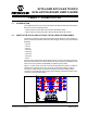
Installation and Operation TP1 TP2 PICkit Serial Interface H1 DIP-8 (1) TP3 1 TP8 SC70-6 (1, 2) 8 TP7 NC VDD VSS SDA SCL NC 7 2 TP6 3 1 6 2 5 3 4 6 TP5 5 4 SOT-23-8 (1, 2) Requires blue wire jumpering to connect the PICkit Interface to the selected device TP4 1 8 2 7 3 6 4 5 R1U TP1 R1D R2U TP2 R2D VDD C1 VSS SOT-23-6 (1, 2) C2 TP1 1 6 TP8 TP2 2 5 TP7 TP3 3 4 TP6 R7U TP7 R7D R8U TP8 R8D Note 1: The SC70 VDD (SOT-23 VSS) signal is connected to the DIP-8 VDD/VS
SC70-6 and SOT-23-6/8 to DIP-8 Evaluation Board User’s Guide 2.3.1 The Hardware Figure 2-2 shows the component layout of the SC70-6 and SOT-23-6/8 to DIP-8 Evaluation Board. This is a small four-layer board (1.43" x 1.255" (36.322 mm x 31.877 mm)). There are ten connection points/pads that can use either through-hole or surface-mount connector posts. The pad labeled VDD is connected to the PCB power plane, while the pad labeled VSS is connected to the PCB ground plane.
Installation and Operation TABLE 2-1: OPTIONAL PASSIVE COMPONENTS (2) Component C1, C2 Power supply bypass capacitors R1U, R2U, R3U, R4U, R5U, R6U, R7U, R8U Pull-up resistor R1D, R2D, R3D, R4D, R5D, R6D, R7D, R8D Pull-down resistor (1) Note 1: 2: 2.4 Comment Whichever pin is the device’s VDD pin, that corresponding RXD footprint can be used for the device’s bypass capacitor. So if Pin 8 is the device’s VDD pin, then install the bypass capacitor in the R8D footprint.
SC70-6 and SOT-23-6/8 to DIP-8 Evaluation Board User’s Guide 2.4.3 Passive Components (RXU, RXD, C1, and C2) The footprints for these components are present to allow maximum flexibility in the use of this PCB to evaluate a wide range of devices. The purpose of these components may vary depending on the device under evaluation and how it is to be used in the desired circuit. Refer to the device data sheet for the recommended components that should be used when evaluating that device.
Installation and Operation 2.4.4.2 SOT-23-6 The 6-pin SOT-23 footprint is laid out for packages that have a typical pitch of 0.65 mm (BSC), a maximum lead width of 0.45 mm, and a maximum molded package width of 1.75 mm. Six lead SOT-23 packages that meet these characteristics should be able to be used with this board. 2.4.4.3 DIP-8 The 8-pin DIP footprint is laid out for packages that have a typical pitch of 100 mil (BSC), a maximum lead width of 22 mil, and a molded package width of 300 mil.
SC70-6 and SOT-23-6/8 to DIP-8 Evaluation Board User’s Guide 2.4.5 PICkit Serial or In-Circuit Serial Programming (ICSP) Interface (Header J1) Figure 2-5 shows the interface connection of Header J1. The VDD and VSS signals are connected to the appropriate power or ground plane. The other four signals are open and can be easily jumpered to any of the eight P1 through P8 connection points.
Installation and Operation 2.4.5.1 PICKIT SERIAL INTERFACE Table 2-2 shows the pin number assignment for the different signals for each of the supported interface protocols (SPI, I2C, etc.) TABLE 2-2: PICKIT SERIAL HEADER SIGNALS PICkit Serial Header Signal Pin Number SPI I2C USART Microwire LIN 1 CS — TX CS TX 2 VDD VDD VDD VDD — 3 VSS VSS VSS VSS VSS 4 SDI SDA — SDI CS/WAKE 5 SCK SCL — SCK FAULT/TXE 6 SDO — RX SDO RX 2.4.5.
SC70-6 and SOT-23-6/8 to DIP-8 Evaluation Board User’s Guide 2.4.6 Evaluating the MCP4018 Device (A Digital Potentiometer with I2C interface) The MCP4018 is a Digital Potentiometer that is in a 6-lead SC70 package with an I2C serial interface. This allows the device to be communicated to (Read and Write) by the PICkit Serial Analyzer. For this to occur, the PICkit Serial Analyzer signals must be connected to the correct MCP4018 signals. These connections are shown in Figure 2-6.
Installation and Operation 2.4.7 Evaluating the MCP41X2 Device (A Digital Potentiometer with SPI interface) The MCP41X2 is a Digital Potentiometer that is in a 8-lead DIP package with an SPI serial interface. This allows the device to be communicated to (Read and Write) by the PICkit Serial Analyzer. For this to occur, the PICkit Serial Analyzer signals must be connected to the correct MCP41X2 signals. These connections are shown in Figure 2-7.
SC70-6 and SOT-23-6/8 to DIP-8 Evaluation Board User’s Guide 2.4.8 The PCB as a SC70, SOT-23 to DIP Socket Converter There may be occasions when it is desirable to convert the footprint of the device to that of a DIP package. This allows the device to be installed into an existing DIP socket. Two 1x4 row pins need to be installed into the PCB’s DIP footprint (on the bottom) when the device is installed into the appropriate package footprint.
SC70-6 AND SOT-23-6/8 TO DIP-8 EVALUATION BOARD USER’S GUIDE Appendix A. Schematic and Layouts A.1 INTRODUCTION This appendix contains the schematics and layouts for the SC70-6 and SOT-23-6/8 to DIP-8 Evaluation Board. Diagrams included in this appendix: • • • • • • A.
SC70-6 and SOT-23-6/8 to DIP-8 Evaluation Board User’s Guide Board - Schematic M A.2.1 DS51874A-page 24 © 2009 Microchip Technology Inc.
Schematic and Layouts A.2.2 Board - Top Trace, Silk and Pads © 2009 Microchip Technology Inc.
SC70-6 and SOT-23-6/8 to DIP-8 Evaluation Board User’s Guide A.2.3 Board - Bottom Trace & Pads DS51874A-page 26 © 2009 Microchip Technology Inc.
Schematic and Layouts A.2.4 Board - Layer 2 Ground Plane © 2009 Microchip Technology Inc.
SC70-6 and SOT-23-6/8 to DIP-8 Evaluation Board User’s Guide A.2.5 Board - Layer 3 Power Plane DS51874A-page 28 © 2009 Microchip Technology Inc.
Schematic and Layouts A.2.6 Board - Bottom Silk, Trace and Pads © 2009 Microchip Technology Inc.
SC70-6 and SOT-23-6/8 to DIP-8 Evaluation Board User’s Guide NOTES: DS51874A-page 30 © 2009 Microchip Technology Inc.
SC70-6 AND SOT-23-6/8 TO DIP-8 EVALUATION BOARD USER’S GUIDE Appendix B.
SC70-6 and SOT-23-6/8 to DIP-8 Evaluation Board User’s Guide NOTES: DS51874A-page 32 © 2009 Microchip Technology Inc.
SC70-6 AND SOT-23-6/8 TO DIP-8 EVALUATION BOARD USER’S GUIDE Appendix C. Board Revision 1 Errata C.1 ISSUE The Revision 1 of this PCB has an issue when the PICkit Serial / ICSP Interface Header (J1) pin 1 is incorrectly assigned to the PICkit Serials pin 6. This means that the orientation marker on the PCB are incorrect for the PICkit Serial Analyzer. C.2 SOLUTION Orientate the PICkit Serial Analyzer pin 1 to the PCB pin 6. Revision 2 of the Schematic and PCB addresses this issue. C.
SC70-6 and SOT-23-6/8 to DIP-8 Evaluation Board User’s Guide Board - Schematic - Revision 1 M C.4.1 DS51874A-page 34 © 2009 Microchip Technology Inc.
Board Revision 1 Errata C.4.2 Board - Revision 1 - Layout Components and Silk © 2009 Microchip Technology Inc.
SC70-6 and SOT-23-6/8 to DIP-8 Evaluation Board User’s Guide C.4.3 Board - Revision 1 - Top Layer and Silk DS51874A-page 36 © 2009 Microchip Technology Inc.
Board Revision 1 Errata C.4.4 Board - Revision 1 - Bottom Layer © 2009 Microchip Technology Inc.
SC70-6 and SOT-23-6/8 to DIP-8 Evaluation Board User’s Guide C.4.5 Board - Revision 1 - Power Plane DS51874A-page 38 © 2009 Microchip Technology Inc.
Board Revision 1 Errata C.4.6 Board - Revision 1 - Ground Plane © 2009 Microchip Technology Inc.
SC70-6 and SOT-23-6/8 to DIP-8 Evaluation Board User’s Guide C.4.7 Board - Revision 1 - Bottom DS51874A-page 40 © 2009 Microchip Technology Inc.
Board Revision 1 Errata NOTES: © 2009 Microchip Technology Inc.
WORLDWIDE SALES AND SERVICE AMERICAS ASIA/PACIFIC ASIA/PACIFIC EUROPE Corporate Office 2355 West Chandler Blvd. Chandler, AZ 85224-6199 Tel: 480-792-7200 Fax: 480-792-7277 Technical Support: http://support.microchip.com Web Address: www.microchip.