
Information


2011-2013 Microchip Technology Inc. DS80000531E-page 5
PIC32MX1XX/2XX
5. Module: ADC
If the ADC module is configured to operate at a
maximum conversion rate of 1.1 Msps, missing
codes are possible every 2
5
codes and the DNL
parameter will not be within the published
specification.
Work around
Configure the ADC module to operate for a
maximum conversion rate of 500 ksps.
Affected Silicon Revisions
6. Module: ADC
If the ADC module is used in conjunction with the
CTMU module in Absolute Capacitive/Time
Measurement mode, Channel 0 positive input
must remain open (CH0SA<3:0> = 1111 or
CH0SB<3:0> = 1111) during the calibration step.
However, open selection for Channel 0 positive
input is not functional and connects this input to
AV
SS.
Work around
Connect the ADC module to any unused pin and
perform the CTMU calibration step. This
connection will add a small amount of additional
capacitance, but will have minimal impact on
overall measurements.
Affected Silicon Revisions
7. Module: ADC
When the ADC module is configured to start
conversion on an external interrupt
(SSRC<2:0> = 001), the start of conversion
always occurs on a rising edge detected at the
INT0 pin, even when the INT0 pin has been
configured to generate an interrupt on a falling
edge (INT0EP = 0).
Work around
Generate ADC conversion triggers on the rising
edge of the INT0 signal.
Alternately, use external circuitry to invert the
signal appearing at the INT0 pin, so that a falling
edge of the input signal is detected as a rising
edge by the INT0 pin.
Affected Silicon Revisions
8. Module: Parallel Master Port (PMP)
If the PMP module is enabled, any pin with a PMP
addressing capability (PMAx) cannot be used as a
general purpose output pin, even when the
corresponding PTEN<10:0> bit in the PMAEN
register is cleared. All other functionality on these
pins, including GPIO input functionality is not
affected.
Work around
To use a GPIO pin as an output when this pin is
shared with PMP addressing functionality and
PMP is enabled, do the following:
1. Enable PMP addressing by setting the
corresponding PTEN<10:0> bit in the
PMAEN register.
2. Instead of using corresponding LATx
registers to output GPIO data, use the
PMADDR register.
Affected Silicon Revisions
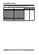
Device Flash
Memory (KB)
Device Silicon Revision
A0 A1
16/32 X X
64/128 X X
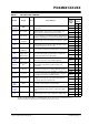
Device Flash
Memory (KB)
Device Silicon Revision
A0 A1
16/32 X X
64/128
Device Flash
Memory (KB)
Device Silicon Revision
A0 A1
16/32 X X
64/128 X X
Device Flash
Memory (KB)
Device Silicon Revision
A0 A1
16/32 X X
64/128 X X