
Information


PIC24F16KL402 FAMILY
DS80000534C-page 4 2011-2013 Microchip Technology Inc.
Data Sheet Clarifications
The following typographic corrections and clarifications
are to be noted for the latest version of the device data
sheet (DS31037B):
1. Module: Front Matter (Device Features)
Under the heading: “Power Management
Modes” on Page 1, the bullet entry for Run
mode current in “Low-Power Consumption” is
corrected to read:
“Run mode current of 150 µA/MHz, 1.8V typical”
2. Module: Pin Diagrams
The pin diagrams for all 20-pin DIP devices
(Pages 4 and 5 of the data sheet) are PDIP
packages, and not Skinny PDIP (SPDIP), as
indicated. SPDIP packaging is not available for
20-pin devices in this device family.
References to SPDIP packaging for 28-pin DIP
devices are corrected as shown.
3. Module: Overview
In Table 1-2 (“Device Features for
PIC24F16KL40X/30X Devices”), references in
the “Packages” row to 20-Pin SPDIP are to be
read as “20-Pin PDIP”. In addition, references to
28-Pin PDIP are to be read as “28-Pin SPDIP”.
In Table 1-3 (“Device Features for the
PIC24F16KL20X/10X Devices”), references in
the “Packages” row to 20-Pin SPDIP are to be
read as “20-Pin PDIP”.
4. Module: I/O Ports
The following is appended to the end of
Section 11.2.1 “Analog Selection Register”:
“On devices which do not have an A/D Con-
verter, it is still necessary to configure the ANSx
registers in order to enable digital input buffers.
Any I/O pins with an ANx function listed in red in
the device pinout diagrams (Pages 3 through 5)
will default to have the digital input buffer
disabled.”
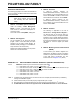
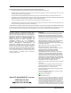
5. Module: Master Synchronous Serial Port
(MSSP)
A new footnote (4) is added to Register 17-3
(SSPxCON1, SPI Mode) to clarify an exception
condition for a particular bit state. The definition
of the state itself is unchanged. The new
footnote is shown in Register 17-3 (below).
REGISTER 17-3: SSPxCON1:MSSPx CONTROL REGISTER 1 (PARTIAL PRESENTATION)
Note: Corrections and additions are shown in
bold. Where possible, the original bold
text formatting has been removed for
clarity.
bit 3-0 SSPM<3:0>: Master Synchronous Serial Port Mode Select bits
(3)
1010 = SPI Master mode, Clock = FOSC/(2 * ([SSPxADD] + 1))
(4)
0101 = SPI Slave mode, Clock = SCKx pin; SSx pin control is disabled, SSx can be used as an I/O pin
0100 = SPI Slave mode, Clock = SCKx pin; SSx pin control is enabled
0011 = SPI Master mode, Clock = TMR2 output/2
0010 = SPI Master mode, Clock = F
OSC/32
0001 = SPI Master mode, Clock = F
OSC/8
0000 = SPI Master mode, Clock = F
OSC/2
Note 1: In Master mode, the overflow bit is not set since each new reception (and transmission) is initiated by
writing to the SSPxBUF register.
2: When enabled, these pins must be properly configured as input or output.
3: Bit combinations not specifically listed here are either reserved or implemented in I
2
C mode only.
4: An SSPxADD value of 00h is not supported when the Baud Rate Generator is used in SPI mode.