
Information


© 2008 Microchip Technology Inc. DS80224E-page 9
PIC18F2525/2620/4525/4620
21. Module: A/D
The A/D offset is greater than the specified limit in
Table 26-24 of the Device Data Sheet. The
updated conditions and limits are shown in bold
text in Table 2.
Work around
Three work arounds exist.
1. Configure the A/D to use the V
REF+ and VREF-
pins for the voltage references. This is done by
setting the VCFG<1:0> bits (ADCON1<5:4>).
2. Perform a conversion on a known voltage
reference voltage and adjust the A/D result in
software.
3. Increase system clock speed to 40 MHz and
adjust A/D settings accordingly. Higher system
clock frequencies decrease offset error.
Date Codes that pertain to this issue:
All engineering and production devices.
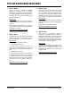
TABLE 2: A/D CONVERTER CHARACTERISTICS: PIC18F2525/2620/4525/4620 (INDUSTRIAL)
PIC18LF2525/2620/4525/4620 (INDUSTRIAL)
22. Module: BOR
The BOR module may reset below the minimum
operating voltage of the device when configured
for BORV1:BORV0 = 11. The updated Reset
voltage specifications are shown in bold in
Table 3.
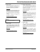
TABLE 3: BROWN-OUT RESET VOLTAGE
Work around
Use the next higher BOR voltage setting to ensure
a low V
DD is detected above 2.0V.
Date Codes that pertain to this issue:
All engineering and production devices.
23. Module: EUSART
The EUSART auto-baud feature may periodically
measure the incoming baud rate incorrectly. The
rate of incorrect baud rate measurements will
depend on the frequency of the incoming
synchronization byte and the system clock
frequency.
Work around
None.
Date Codes that pertain to this issue:
All engineering and production devices.
24. Module: EUSART
In Synchronous mode (SYNC = 1) with clock
polarity high (SCKP = 1), the EUSART transmits a
shorter than expected clock on the CK pin for bit 0.
Work around
None.
Date Codes that pertain to this issue:
All engineering and production devices.
Param
No.
Symbol Characteristic Min Typ Max Units Conditions
A06A E
OFF Offset Error — — <±2.0 LSb VREF = VREF+ and VREF-
A06 E
OFF Offset Error — — <±3.5 LSb VREF = VSS and VDD
Param
No.
Sym Characteristic Min Typ Max Unit
D005 V
BOR Brown-out Reset Voltage
PIC18LF2525/2620/4525/4620
BORV1:BORV0 =
11 N/A 2.05 N/A V