
Information


© 2008 Microchip Technology Inc. DS80224E-page 11
PIC18F2525/2620/4525/4620
31. Module: MSSP
In SPI mode, the Buffer Full flag (BF bit in the
SSPSTAT register), the Write Collision Detect bit
(WCOL bit in SSPCON1) and the Receive
Overflow Indicator bit (SSPOV in SSPCON1) are
not reset upon disabling the SPI module (by
clearing the SSPEN bit in the SSPCON1 register).
For example, if SSPBUF is full (BF bit is set) and
the MSSP module is disabled and re-enabled, the
BF bit will remain set. In SPI Slave mode, a sub-
sequent write to SSPBUF will result in a write
collision. Also, if a new byte is received, a receive
overflow will occur.
Work around
Ensure that if the buffer is full, SSPBUF is read
(thus clearing the BF flag) and WCOL is clear
before disabling the MSSP module. If the module
is configured in SPI Slave mode, ensure that the
SSPOV bit is clear before disabling the module.
Date Codes that pertain to this issue:
All engineering and production devices.
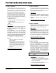
32. Module: MSSP (SPI Mode)
When the SPI is using Timer2/2 as the clock
source, a shorter than expected SCK pulse may
occur on the first bit of the transmitted/received
data (Figure 1).
FIGURE 1: SCK PULSE VARIATION
USING TIMER2/2
Work around
To avoid producing the short pulse, turn off Timer2
and clear the TMR2 register, load the SSPBUF
with the data to transmit and then turn Timer2 back
on. Refer to Example 5 for sample code.
EXAMPLE 5: AVOIDING THE INITIAL
SHORT SCK PULSE
Date Codes that pertain to this issue:
All engineering and production devices.
SDO
SCK
Write SSPBUF
bit 0 =
1
bit 1 =
0
bit 2 =
1
. . . .
LOOP BTFSS SSPSTAT, BF ;Data received?
;(Xmit complete?)
BRA LOOP ;No
MOVF SSPBUF, W ;W = SSPBUF
MOVWF RXDATA ;Save in user RAM
MOVF TXDATA, W ;W = TXDATA
BCF T2CON, TMR2ON ;Timer2 off
CLRF TMR2 ;Clear Timer2
MOVWF SSPBUF ;Xmit New data
BSF T2CON, TMR2ON ;Timer2 on