
Information


Table Of Contents
- Clarifications/Corrections to the Data Sheet:
- 1. Module: Timer1 Module
- 2. Module: Timer1 Module
- 3. Module: Universal Serial Bus (USB)
- 4. Module: Master Synchronous Serial Port (MSSP) Module
- 5. Module: 10-Bit Analog-to-Digital (A/D) Converter Module
- 6. Module: Special Features of the CPU
- 7. Module: Electrical Characteristics
- 8. Module: Electrical Characteristics
- 9. Module: Electrical Characteristics
- Revision History
- Worldwide Sales and Service
© 2006 Microchip Technology Inc. DS80278A-page 3
PIC18F2455/2550/4455/4550
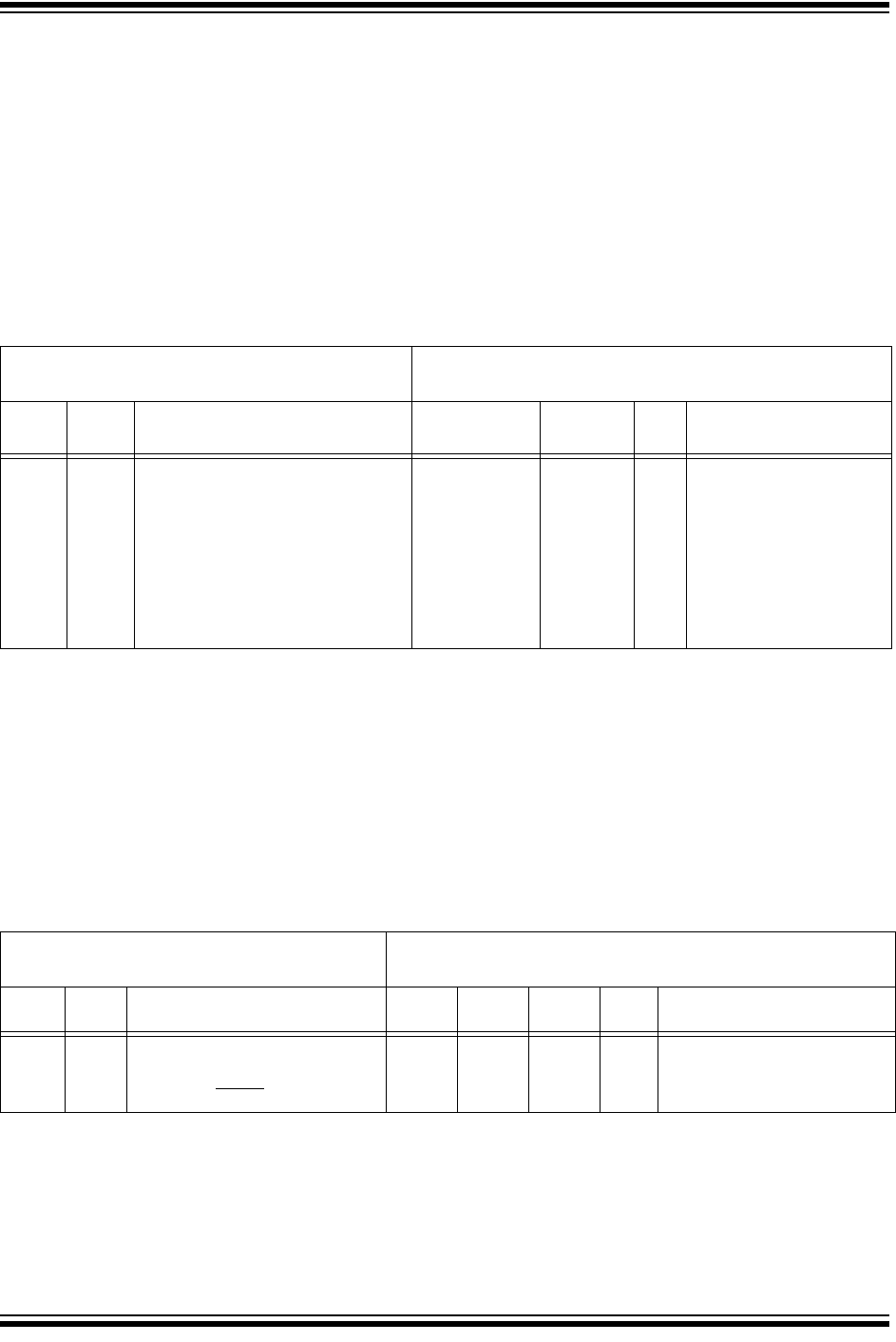
7. Module: Electrical Characteristics
In Section 28.3 “DC Characteristics,” pin-
specific variations of parameters D031 (Input Low
Voltage) and D041 (Input High Voltage) are cor-
rected as characteristic for pins RB0 and RB1, not
pins RC3 and RC4.
The following relevant portion of the table indicates
the corrections. (For clarity, the corrected items
appear in bold text – all other text appears in plain
text for purposes of this errata.)
8. Module: Electrical Characteristics
In “Table 28-1: Memory Programming Require-
ments,” the symbol for parameter D110 is
corrected to VIHH, rather than VPP.
The following relevant portion of Table 28-1 indi-
cates the correction. (For clarity, the corrected item
appears in bold text – all other text appears in
plain text for purposes of this errata.)
TABLE 28-1: MEMORY PROGRAMMING REQUIREMENTS (PARTIAL PRESENTATION)
28.3 DC Characteristics: PIC18F2455/2550/4455/4550 (Industrial)
PIC18LF2455/2550/4455/4550 (Industrial) (Partial Presentation)
DC CHARACTERISTICS
Standard Operating Conditions (unless otherwise stated)
Operating temperature -40°C ≤ T
A ≤ +85°C for industrial
Param
No.
Symbol Characteristic Min Max Units Conditions
V
IL Input Low Voltage
D031
with Schmitt Trigger buffer
RB0 and RB1
V
SS
VSS
0.2 VDD
0.3 VDD
V
V
V
IH Input High Voltage
D041
with Schmitt Trigger buffer
RB0 and RB1
0.8 V
DD
0.7 VDD
VDD
VDD
V
V
DC Characteristics
Standard Operating Conditions (unless otherwise stated)
Operating temperature -40°C ≤ TA ≤ +85°C for industrial
Param
No.
Sym Characteristic Min Typ† Max Units Conditions
Internal Program Memory
Programming Specifications(1)
D110
V
IHH Voltage on MCLR/VPP/RE3 pin 9.00 — 13.25 V (Note 2)
† Data in “Typ” column is at 5.0V, 25°C unless otherwise stated. These parameters are for design guidance
only and are not tested.
Note 1: These specifications are for programming the on-chip program memory through the use of table write
instructions.
2: Required only if Single-Supply Programming is disabled.