
Datasheet


PIC18F87K22 FAMILY
DS39960D-page 514 2011 Microchip Technology Inc.
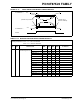
FIGURE 31-14: EXAMPLE SPI MASTER MODE TIMING (CKE = 0)
TABLE 31-17: EXAMPLE SPI MODE REQUIREMENTS (MASTER MODE, CKE = 0)
Param
No.
Symbol Characteristic Min Max Units Conditions
73 TDIV2SCH,
T
DIV2SCL
Setup Time of SDIx Data Input to SCKx Edge 20 — ns
73A T
B2B Last Clock Edge of Byte 1 to the 1st Clock Edge
of Byte 2
1.5 TCY + 40 — ns
74 T
SCH2DIL,
T
SCL2DIL
Hold Time of SDIx Data Input to SCKx Edge 40 — ns
75 T
DOR SDOx Data Output Rise Time — 25 ns
76 T
DOF SDOx Data Output Fall Time — 25 ns
78 T
SCR SCKx Output Rise Time (Master mode) — 25 ns
79 T
SCF SCKx Output Fall Time (Master mode) — 25 ns
80 T
SCH2DOV,
T
SCL2DOV
SDOx Data Output Valid after SCKx Edge — 50 ns
SCKx
(CKPx =
0)
SCKx
(CKPx =
1)
SDOx
SDIx
73
74
75, 76
78
79
80
79
78
MSb LSb
bit 6 - - - - - - 1
LSb In
bit 6 - - - - 1
Note: Refer to Figure 31-3 for load conditions.
MSb In