
Datasheet


2010 Microchip Technology Inc. DS41303G-page 61
PIC18F2XK20/4XK20
ADRESH
PIC18F2XK20 PIC18F4XK20
xxxx xxxx uuuu uuuu uuuu uuuu
ADRESL
PIC18F2XK20 PIC18F4XK20
xxxx xxxx uuuu uuuu uuuu uuuu
ADCON0
PIC18F2XK20 PIC18F4XK20
--00 0000 --00 0000 --uu uuuu
ADCON1
PIC18F2XK20 PIC18F4XK20
--00 0qqq --00 0qqq --uu uuuu
ADCON2
PIC18F2XK20 PIC18F4XK20
0-00 0000 0-00 0000 u-uu uuuu
CCPR1H
PIC18F2XK20 PIC18F4XK20
xxxx xxxx uuuu uuuu uuuu uuuu
CCPR1L
PIC18F2XK20 PIC18F4XK20
xxxx xxxx uuuu uuuu uuuu uuuu
CCP1CON
PIC18F2XK20 PIC18F4XK20
0000 0000 0000 0000 uuuu uuuu
CCPR2H
PIC18F2XK20 PIC18F4XK20
xxxx xxxx uuuu uuuu uuuu uuuu
CCPR2L
PIC18F2XK20 PIC18F4XK20
xxxx xxxx uuuu uuuu uuuu uuuu
CCP2CON
PIC18F2XK20 PIC18F4XK20
--00 0000 --00 0000 --uu uuuu
PSTRCON
PIC18F2XK20 PIC18F4XK20
---0 0001 ---0 0001 ---u uuuu
BAUDCON
PIC18F2XK20 PIC18F4XK20
0100 0-00 0100 0-00 uuuu u-uu
PWM1CON
PIC18F2XK20 PIC18F4XK20
0000 0000 0000 0000 uuuu uuuu
ECCP1AS
PIC18F2XK20 PIC18F4XK20
0000 0000 0000 0000 uuuu uuuu
CVRCON
PIC18F2XK20 PIC18F4XK20
0000 0000 0000 0000 uuuu uuuu
CVRCON2
PIC18F2XK20 PIC18F4XK20
00-- ---- 00-- ---- uu-- ----
TMR3H
PIC18F2XK20 PIC18F4XK20
xxxx xxxx uuuu uuuu uuuu uuuu
TMR3L
PIC18F2XK20 PIC18F4XK20
xxxx xxxx uuuu uuuu uuuu uuuu
T3CON
PIC18F2XK20 PIC18F4XK20
0000 0000 uuuu uuuu uuuu uuuu
SPBRGH
PIC18F2XK20 PIC18F4XK20
0000 0000 0000 0000 uuuu uuuu
SPBRG
PIC18F2XK20 PIC18F4XK20
0000 0000 0000 0000 uuuu uuuu
RCREG
PIC18F2XK20 PIC18F4XK20
0000 0000 0000 0000 uuuu uuuu
TXREG
PIC18F2XK20 PIC18F4XK20
0000 0000 0000 0000 uuuu uuuu
TXSTA
PIC18F2XK20 PIC18F4XK20
0000 0010 0000 0010 uuuu uuuu
RCSTA
PIC18F2XK20 PIC18F4XK20
0000 000x 0000 000x uuuu uuuu
EEADR
PIC18F2XK20 PIC18F4XK20
0000 0000 0000 0000 uuuu uuuu
EEADRH
PIC18F26K20 PIC18F46K20
---- --00 ---- --00 ---- --uu
EEDATA
PIC18F2XK20 PIC18F4XK20
0000 0000 0000 0000 uuuu uuuu
EECON2
PIC18F2XK20 PIC18F4XK20
0000 0000 0000 0000 0000 0000
EECON1
PIC18F2XK20 PIC18F4XK20
xx-0 x000 uu-0 u000 uu-0 u000
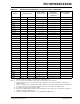
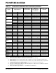
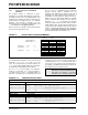
TABLE 4-4: INITIALIZATION CONDITIONS FOR ALL REGISTERS (CONTINUED)
Register Applicable Devices
Power-on Reset,
Brown-out Reset
MCLR
Resets,
WDT Reset,
RESET Instruction,
Stack Resets
Wake-up via WDT
or Interrupt
Legend: u = unchanged, x = unknown, - = unimplemented bit, read as ‘0’, q = value depends on condition.
Shaded cells indicate conditions do not apply for the designated device.
Note 1: One or more bits in the INTCONx or PIRx registers will be affected (to cause wake-up).
2: When the wake-up is due to an interrupt and the GIEL or GIEH bit is set, the PC is loaded with the interrupt vector
(0008h or 0018h).
3: When the wake-up is due to an interrupt and the GIEL or GIEH bit is set, the TOSU, TOSH and TOSL are updated with
the current value of the PC. The STKPTR is modified to point to the next location in the hardware stack.
4: See Table 4-3 for Reset value for specific condition.
5: Bits 6 and 7 of PORTA, LATA and TRISA are enabled, depending on the oscillator mode selected. When not enabled as
PORTA pins, they are disabled and read ‘0’.
6: All bits of the ANSELH register initialize to ‘0’ if the PBADEN bit of CONFIG3H is ‘0’.