
Datasheet


2010 Microchip Technology Inc. DS41303G-page 391
PIC18F2XK20/4XK20
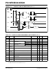
FIGURE 26-11: PARALLEL SLAVE PORT TIMING (PIC18F4XK20)
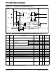
TABLE 26-13: PARALLEL SLAVE PORT REQUIREMENTS (PIC18F4XK20)
Note: Refer to Figure 26-4 for load conditions.
RE2/CS
RE0/RD
RE1/WR
RD7:RD0
62
63
64
65
Param.
No.
Symbol Characteristic Min Max Units Conditions
62 TdtV2wrH Data In Valid before WR
or CS
(setup time)
20 — ns
63 TwrH2dtI WR
or CS to Data–In Invalid (hold time) 20 — ns
64 TrdL2dtV RD
and CS to Data–Out Valid — 80 ns
65 TrdH2dtI RD
or CS to Data–Out Invalid 10 30 ns
66 TibfINH Inhibit of the IBF Flag bit being Cleared from
WR
or CS
—3 T
CY