
Datasheet


2010 Microchip Technology Inc. DS41303G-page 385
PIC18F2XK20/4XK20
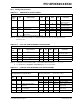
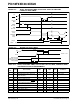
TABLE 26-6: EXTERNAL CLOCK TIMING REQUIREMENTS
Param.
No.
Symbol Characteristic Min Max Units Conditions
1A F
OSC External CLKIN
Frequency
(1)
DC 48 MHz EC, ECIO Oscillator mode,
(Extended Range Devices)
DC 64 MHz EC, ECIO Oscillator mode,
(Industrial Range Devices)
Oscillator Frequency
(1)
DC 4 MHz RC Oscillator mode
0.1 4 MHz XT Oscillator mode
4 25 MHz HS Oscillator mode
4 16 MHz HS + PLL Oscillator mode,
(Industrial Range Devices)
4 12 MHz HS + PLL Oscillator mode,
(Extended Range Devices)
5 200 kHz LP Oscillator mode
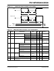
1T
OSC External CLKIN Period
(1)
20.8 — ns EC, ECIO, Oscillator mode
(Extended Range Devices)
15.6 — ns EC, ECIO, Oscillator mode,
(Industrial Range Devices)
Oscillator Period
(1)
250 — ns RC Oscillator mode
250 10,000 ns XT Oscillator mode
40
62.5
83.3
250
250
250
ns
ns
ns
HS Oscillator mode
HS + PLL Oscillator mode,
(Industrial range devices)
HS + PLL Oscillator mode,
(Extended Range Devices)
5200s LP Oscillator mode
2T
CY Instruction Cycle Time
(1)
62.5 — ns TCY = 4/FOSC
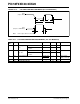
3TOSL,
T
OSH
External Clock in (OSC1)
High or Low Time
30 — ns XT Oscillator mode
2.5 — s LP Oscillator mode
10 — ns HS Oscillator mode
4T
OSR,
T
OSF
External Clock in (OSC1)
Rise or Fall Time
— 20 ns XT Oscillator mode
— 50 ns LP Oscillator mode
— 7.5 ns HS Oscillator mode
Note 1: Instruction cycle period (T
CY) equals four times the input oscillator time base period for all configurations
except PLL. All specified values are based on characterization data for that particular oscillator type under
standard operating conditions with the device executing code. Exceeding these specified limits may result
in an unstable oscillator operation and/or higher than expected current consumption. All devices are tested
to operate at “min.” values with an external clock applied to the OSC1/CLKIN pin. When an external clock
input is used, the “max.” cycle time limit is “DC” (no clock) for all devices.