
Datasheet


2010 Microchip Technology Inc. DS41303G-page 371
PIC18F2XK20/4XK20
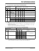
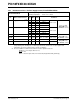
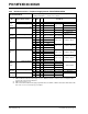
26.1 DC Characteristics:Supply Voltage, PIC18F2XK20/4XK20
PIC18F2XK20/4XK20
Standard Operating Conditions (unless otherwise stated)
Operating temperature -40°C T
A +125°C
Param
No.
Symbol Characteristic Min Typ Max Units Conditions
D001 V
DD Supply Voltage
1.8 — 3.6 V
D002 V
DR RAM Data Retention
Voltage
(1)
1.5 — — V
D003 V
POR VDD Start Voltage
to ensure internal
Power-on Reset signal
— — 0.7 V See section on Power-on Reset for details
D004 SVDD VDD Rise Rate
to ensure internal
Power-on Reset signal
0.05 — — V/ms See section on Power-on Reset for details
D005 VBOR Brown-out Reset Voltage
BORV<1:0> = 11
(2)
1.72 1.82 1.95 V
BORV<1:0> = 10 2.15 2.27 2.40 V
BORV<1:0> = 01 2.65 2.75 2.90 V
BORV<1:0> = 00
(3)
2.98 3.08 3.25 V
Note 1: This is the limit to which VDD can be lowered in Sleep mode, or during a device Reset, without losing RAM
data.
2: With BOR enabled, operation is supported until a BOR occurs. This is valid although V
DD may be below the
minimum rated supply voltage.
3: With BOR enabled, full-speed operation (F
OSC = 64 MHZ) is supported until a BOR occurs. This is valid
although V
DD may be below the minimum voltage for this frequency.
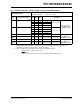
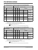
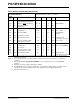
26.2 DC Characteristics: Power-Down Current, PIC18F2XK20/4XK20
PIC18F2XK20/4XK20
Standard Operating Conditions (unless otherwise stated)
Operating temperature -40°C TA +125°C
Param
No.
Device Characteristics Typ Max Units Conditions
D006 Power-down Current (I
PD)
(1)
0.05 1.0 A -40°C
V
DD = 1.8V, (Sleep mode)
0.05 1.0 A+25°C
0.6 3.0 A+85°C
420A +125°C
D007 0.1 1.0 A -40°C
V
DD = 3.0V, (Sleep mode)
0.1 1.0 A+25°C
0.7 3.0 A+85°C
520A +125°C
Note 1: The power-down current in Sleep mode does not depend on the oscillator type. Power-down current is
measured with the part in Sleep mode, with all I/O pins in high-impedance state and tied to V
DD or VSS and
all features that add delta current disabled (such as WDT, Timer1 Oscillator, BOR, etc.).