
Datasheet


2010 Microchip Technology Inc. DS41303G-page 303
PIC18F2XK20/4XK20
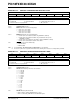
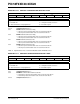
REGISTER 23-4: CONFIG3H: CONFIGURATION REGISTER 3 HIGH
R/P-1 U-0 U-0 U-0 R/P-1 R/P-0 R/P-1 R/P-1
MCLRE — — — HFOFST LPT1OSC PBADEN CCP2MX
bit 7 bit 0
Legend:
R = Readable bit P = Programmable bit U = Unimplemented bit, read as ‘0’
-n = Value when device is unprogrammed x = Bit is unknown
bit 7 MCLRE: MCLR
Pin Enable bit
1 = MCLR
pin enabled; RE3 input pin disabled
0 = RE3 input pin enabled; MCLR
disabled
bit 6-4 Unimplemented: Read as ‘0’
bit 3 HFOFST: HFINTOSC Fast Start-up
1 = HFINTOSC starts clocking the CPU without waiting for the oscillator to stabilize.
0 = The system clock is held off until the HFINTOSC is stable.
bit 2 LPT1OSC: Low-Power Timer1 Oscillator Enable bit
1 = Timer1 configured for low-power operation
0 = Timer1 configured for higher power operation
bit 1 PBADEN: PORTB A/D Enable bit
(Affects ANSELH Reset state. ANSELH controls PORTB<4:0> pin configuration.)
1 = PORTB<4:0> pins are configured as analog input channels on Reset
0 = PORTB<4:0> pins are configured as digital I/O on Reset
bit 0 CCP2MX: CCP2 MUX bit
1 = CCP2 input/output is multiplexed with RC1
0 = CCP2 input/output is multiplexed with RB3
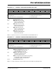
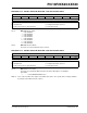
REGISTER 23-5: CONFIG4L: CONFIGURATION REGISTER 4 LOW
R/P-1 R/P-0 U-0 U-0 U-0 R/P-1 U-0
R/P-1
DEBUG XINST — — —LVP
(1)
—
STVREN
bit 7
bit 0
Legend:
R = Readable bit P = Programmable bit U = Unimplemented bit, read as ‘0’
-n = Value when device is unprogrammed x = Bit is unknown
bit 7 DEBUG
: Background Debugger Enable bit
1 = Background debugger disabled, RB6 and RB7 configured as general purpose I/O pins
0 = Background debugger enabled, RB6 and RB7 are dedicated to In-Circuit Debug
bit 6 XINST: Extended Instruction Set Enable bit
1 = Instruction set extension and Indexed Addressing mode enabled
0 = Instruction set extension and Indexed Addressing mode disabled (Legacy mode)
bit 5-3 Unimplemented: Read as ‘0’
bit 2 LVP: Single-Supply ICSP Enable bit
1 = Single-Supply ICSP enabled
0 = Single-Supply ICSP disabled
bit 1 Unimplemented: Read as ‘0’
bit 0 STVREN: Stack Full/Underflow Reset Enable bit
1 = Stack full/underflow will cause Reset
0 = Stack full/underflow will not cause Reset
Note 1: Can only be changed by a programmer in high-voltage programming mode.