
Datasheet

PIC18F2XK20/4XK20
DS41303G-page 20 2010 Microchip Technology Inc.
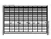
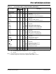
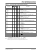
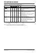
TABLE 1-3: PIC18F4XK20 PINOUT I/O DESCRIPTIONS
Pin Name
Pin Number
Pin
Type
Buffer
Type
Description
PDIP QFN TQFP
MCLR
/VPP/RE3
MCLR
VPP
RE3
11818
I
P
I
ST
ST
Master Clear (input) or programming voltage (input)
Active-low Master Clear (device Reset) input
Programming voltage input
Digital input
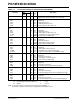
OSC1/CLKIN/RA7
OSC1
CLKIN
RA7
13 32 30
I
I
I/O
ST
CMOS
TTL
Oscillator crystal or external clock input
Oscillator crystal input or external clock source input
ST buffer when configured in RC mode;
analog otherwise
External clock source input. Always associated with
pin function OSC1 (See related OSC1/CLKIN,
OSC2/CLKOUT pins)
General purpose I/O pin
OSC2/CLKOUT/RA6
OSC2
CLKOUT
RA6
14 33 31
O
O
I/O
—
—
TTL
Oscillator crystal or clock output
Oscillator crystal output. Connects to crystal
or resonator in Crystal Oscillator mode
In RC mode, OSC2 pin outputs CLKOUT which
has 1/4 the frequency of OSC1 and denotes
the instruction cycle rate
General purpose I/O pin
Legend: TTL = TTL compatible input CMOS = CMOS compatible input or output
ST = Schmitt Trigger input with CMOS levels I = Input
O = Output P = Power
Note 1: Default assignment for CCP2 when Configuration bit CCP2MX is set.
2: Alternate assignment for CCP2 when Configuration bit CCP2MX is cleared.