
Datasheet


2010 Microchip Technology Inc. DS41303G-page 157
PIC18F2XK20/4XK20
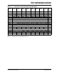
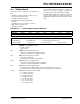
FIGURE 12-2: TIMER0 BLOCK DIAGRAM (16-BIT MODE)
12.3 Prescaler
An 8-bit counter is available as a prescaler for the Timer0
module. The prescaler is not directly readable or writable;
its value is set by the PSA and T0PS<2:0> bits of the
T0CON register which determine the prescaler
assignment and prescale ratio.
Clearing the PSA bit assigns the prescaler to the
Timer0 module. When the prescaler is assigned,
prescale values from 1:2 through 1:256 in integer
power-of-2 increments are selectable.
When assigned to the Timer0 module, all instructions
writing to the TMR0 register (e.g., CLRF TMR0, MOVWF
TMR0, BSF TMR0, etc.) clear the prescaler count.
12.3.1 SWITCHING PRESCALER
ASSIGNMENT
The prescaler assignment is fully under software
control and can be changed “on-the-fly” during program
execution.
12.4 Timer0 Interrupt
The TMR0 interrupt is generated when the TMR0 reg-
ister overflows from FFh to 00h in 8-bit mode, or from
FFFFh to 0000h in 16-bit mode. This overflow sets the
TMR0IF flag bit. The interrupt can be masked by clear-
ing the TMR0IE bit of the INTCON register. Before
re-enabling the interrupt, the TMR0IF bit must be
cleared by software in the Interrupt Service Routine.
Since Timer0 is shut down in Sleep mode, the TMR0
interrupt cannot awaken the processor from Sleep.
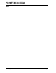
TABLE 12-1: REGISTERS ASSOCIATED WITH TIMER0
Note: Upon Reset, Timer0 is enabled in 8-bit mode with clock input from T0CKI max. prescale.
T0CKI pin
T0SE
0
1
0
1
T0CS
FOSC/4
Programmable
Prescaler
Sync with
Internal
Clocks
TMR0L
(2 TCY Delay)
Internal Data Bus
8
PSA
T0PS<2:0>
Set
TMR0IF
on Overflow
3
TMR0
TMR0H
High Byte
8
8
8
Read TMR0L
Write TMR0L
8
Note: Writing to TMR0 when the prescaler is
assigned to Timer0 will clear the prescaler
count but will not change the prescaler
assignment.
Name Bit 7 Bit 6 Bit 5 Bit 4 Bit 3 Bit 2 Bit 1 Bit 0
Reset
Values
on page
TMR0L Timer0 Register, Low Byte 60
TMR0H Timer0 Register, High Byte 60
INTCON GIE/GIEH PEIE/GIEL TMR0IE INT0IE RBIE TMR0IF INT0IF RBIF 59
T0CON TMR0ON T08BIT T0CS T0SE PSA T0PS2 T0PS1 T0PS0 60
TRISA RA7
(1)
RA6
(1)
RA5 RA4 RA3 RA2 RA1 RA0 62
Legend: Shaded cells are not used by Timer0.
Note 1: PORTA<7:6> and their direction bits are individually configured as port pins based on various primary
oscillator modes. When disabled, these bits read as ‘0’.