PIC18F23K20/24K20/25K20/26K20/ 43K20/44K20/45K20/46K20 Data Sheet 28/40/44-Pin Flash Microcontrollers with nanoWatt XLP Technology 2010 Microchip Technology Inc.
Note the following details of the code protection feature on Microchip devices: • Microchip products meet the specification contained in their particular Microchip Data Sheet. • Microchip believes that its family of products is one of the most secure families of its kind on the market today, when used in the intended manner and under normal conditions. • There are dishonest and possibly illegal methods used to breach the code protection feature.
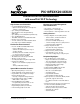
PIC18F2XK20/4XK20 28/40/44-Pin Flash Microcontrollers with nanoWatt XLP Technology High-Performance RISC CPU: • C Compiler Optimized Architecture: - Optional extended instruction set designed to optimize re-entrant code • Up to 1024 bytes Data EEPROM • Up to 64 Kbytes Linear Program Memory Addressing • Up to 3936 bytes Linear Data Memory Addressing • Up to 16 MIPS Operation • 16-bit Wide Instructions, 8-bit Wide Data Path • Priority Levels for Interrupts • 31-Level, Software Accessible Hardware Stack • 8 x
PIC18F2XK20/4XK20 Program Memory Device Data Memory (1) Flash # Single-Word SRAM EEPROM I/O (bytes) Instructions (bytes) (bytes) 10-bit A/D (ch)(2) CCP/ ECCP (PWM) MSSP SPI Master I2C™ EUSART - Comp.
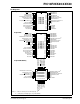
PIC18F2XK20/4XK20 Pin Diagrams 28-pin PDIP, SOIC, SSOP 1 2 3 4 5 6 7 8 9 10 11 12 13 14 15 16 17 18 19 20 RA1/AN1/C12IN1RA0/AN0/C12IN0- MCLR/VPP/RE3 RA0/AN0/C12IN0RA1/AN1/C12IN1RA2/AN2/VREF-/CVREF/C2IN+ RA3/AN3/VREF+/C1IN+ RA4/T0CKI/C1OUT RA5/AN4/SS/HLVDIN/C2OUT RE0/RD/AN5 RE1/WR/AN6 RE2/CS/AN7 VDD VSS OSC1/CLKIN/RA7 OSC2/CLKOUT/RA6 RC0/T1OSO/T13CKI RC1/T1OSI/CCP2(1) RC2/CCP1/P1A RC3/SCK/SCL RD0/PSP0 RD1/PSP1 PIC18F43K20 PIC18F44K20 PIC18F45K20 PIC18F46K20 40-pin PDIP 28-pin QFN/UQFN(2) 28 27 26 25 2
PIC18F2XK20/4XK20 RC6/TX/CK RC5/SDO RC4/SDI/SDA RD3/PSP3 RD2/PSP2 RD1/PSP1 RD0/PSP0 RC3/SCK/SCL RC2/CCP1/P1A RC1/T1OSI/CCP2(1) NC Pin Diagrams (Cont.
PIC18F2XK20/4XK20 RA2 AN2 C2IN+ VREF-/ CVREF 5 22 22 RA3 AN3 6 23 23 RA4 C1IN+ VREF+ C1OUT — DIL Pin Basic 21 Pull-up 21 Interrupts 4 Slave — — Timers C12IN1- MSSP C12IN0- AN1 EUSART AN0 RA1 ECCP RA0 20 Analog 19 20 I/O 19 3 QFN Pin 2 TQFP Pin Reference PIC18F4XK20 PIN SUMMARY Comparator TABLE 1: — — — — — — — — — — — — — — — — — — — — — — — — — — — — — — — — — — — T0CKI — — — — — — — — — — — — — — — — — — — — — — — — — — — — — — — — — — —
PIC18F2XK20/4XK20 AN2 C2IN+ VREF-/ CVREF AN3 C1IN+ VREF+ Basic RA2 Pull-up 1 Interrupts C12IN1- 4 Slave C12IN0- AN1 Timers AN0 RA1 MSSP Comparator RA0 28 EUSART Analog 27 3 ECCP I/O 2 Reference Pin QUAD PIC18F2XK20 PIN SUMMARY Pin DIL TABLE 2: 5 2 RA3 6 3 RA4 7 4 RA5 10 7 RA6 OSC2/ CLKOUT 9 6 RA7 OSC1/ CLKIN C1OUT AN4 21 18 RB0 AN12 22 19 RB1 AN10 23 20 RB2 AN8 24 21 RB3 AN9 25 22 RB4 AN11 C2OUT C12IN3C12IN2- T0CKI HLVDIN SS FLT0
PIC18F2XK20/4XK20 Table of Contents 1.0 Device Overview ....................................................................................................................................................................... 11 2.0 Oscillator Module (With Fail-Safe Clock Monitor)...................................................................................................................... 27 3.0 Power-Managed Modes .......................................................................................
PIC18F2XK20/4XK20 TO OUR VALUED CUSTOMERS It is our intention to provide our valued customers with the best documentation possible to ensure successful use of your Microchip products. To this end, we will continue to improve our publications to better suit your needs. Our publications will be refined and enhanced as new volumes and updates are introduced. If you have any questions or comments regarding this publication, please contact the Marketing Communications Department via E-mail at docerrors@mail.
PIC18F2XK20/4XK20 1.0 DEVICE OVERVIEW This document contains device specific information for the following devices: • PIC18F23K20 • PIC18F43K20 • PIC18F24K20 • PIC18F44K20 • PIC18F25K20 • PIC18F45K20 • PIC18F26K20 • PIC18F46K20 This family offers the advantages of all PIC18 microcontrollers – namely, high computational performance at an economical price – with the addition of high-endurance, Flash program memory.
PIC18F2XK20/4XK20 1.2 Other Special Features • Memory Endurance: The Flash cells for both program memory and data EEPROM are rated to last for many thousands of erase/write cycles – up to 10K for program memory and 100K for EEPROM. Data retention without refresh is conservatively estimated to be greater than 40 years. • Self-programmability: These devices can write to their own program memory spaces under internal software control.
2010 Microchip Technology Inc.
PIC18F2XK20/4XK20 FIGURE 1-1: PIC18F2XK20 (28-PIN) BLOCK DIAGRAM Data Bus<8> Table Pointer<21> Data Latch 8 8 inc/dec logic PORTA Data Memory PCLATU PCLATH 21 Address Latch 20 PCU PCH PCL Program Counter 12 Data Address<12> RA0/AN0 RA1/AN1 RA2/AN2/VREF-/CVREF RA3/AN3/VREF+ RA4/T0CKI/C1OUT RA5/AN4/SS/HLVDIN/C2OUT OSC2/CLKOUT(3)/RA6 OSC1/CLKIN(3)/RA7 31-Level Stack 4 BSR Address Latch Program Memory (8/16/32/64 Kbytes) STKPTR 12 FSR0 FSR1 FSR2 Data Latch 4 Access Bank 12 PORTB 8 inc/dec lo
PIC18F2XK20/4XK20 FIGURE 1-2: PIC18F4XK20 (40/44-PIN) BLOCK DIAGRAM Data Bus<8> PORTA Table Pointer<21> RA0/AN0 RA1/AN1 RA2/AN2/VREF-/CVREF RA3/AN3/VREF+ RA4/T0CKI/C1OUT RA5/AN4/SS/HLVDIN/C2OUT OSC2/CLKOUT(3)/RA6 OSC1/CLKIN(3)/RA7 Data Latch 8 8 inc/dec logic Data Memory PCLATU PCLATH 21 Address Latch 20 PCU PCH PCL Program Counter 12 Data Address<12> PORTB 31-Level Stack 4 BSR Address Latch Program Memory (8/16/32/64 Kbytes) STKPTR FSR0 FSR1 FSR2 Data Latch 8 RB0/INT0/FLT0/AN12 RB1/INT1/
PIC18F2XK20/4XK20 TABLE 1-2: PIC18F2XK20 PINOUT I/O DESCRIPTIONS Pin Number Pin Name Pin Buffer PDIP, QFN Type Type SOIC MCLR/VPP/RE3 MCLR VPP RE3 1 OSC1/CLKIN/RA7 OSC1 9 26 I P I 6 ST ST ST O — CLKOUT O — RA6 I/O TTL RA7 OSC2/CLKOUT/RA6 OSC2 10 Master Clear (input) or programming voltage (input) Active-low Master Clear (device Reset) input Programming voltage input Digital input Oscillator crystal or external clock input Oscillator crystal input or external clock source input ST buffer
PIC18F2XK20/4XK20 TABLE 1-2: PIC18F2XK20 PINOUT I/O DESCRIPTIONS (CONTINUED) Pin Name Pin Number Pin Buffer PDIP, QFN Type Type SOIC Description PORTA is a bidirectional I/O port.
PIC18F2XK20/4XK20 TABLE 1-2: PIC18F2XK20 PINOUT I/O DESCRIPTIONS (CONTINUED) Pin Name Pin Number Pin Buffer PDIP, QFN Type Type SOIC Description PORTB is a bidirectional I/O port. PORTB can be software programmed for internal weak pull-up on each input.
PIC18F2XK20/4XK20 TABLE 1-2: PIC18F2XK20 PINOUT I/O DESCRIPTIONS (CONTINUED) Pin Name Pin Number Pin Buffer PDIP, QFN Type Type SOIC Description PORTC is a bidirectional I/O port.
PIC18F2XK20/4XK20 TABLE 1-3: PIC18F4XK20 PINOUT I/O DESCRIPTIONS Pin Name Pin Number PDIP MCLR/VPP/RE3 MCLR VPP RE3 1 OSC1/CLKIN/RA7 OSC1 13 Pin Buffer QFN TQFP Type Type 18 18 I P I 32 30 I CLKIN I RA7 OSC2/CLKOUT/RA6 OSC2 I/O 14 33 ST ST Description Master Clear (input) or programming voltage (input) Active-low Master Clear (device Reset) input Programming voltage input Digital input Oscillator crystal or external clock input Oscillator crystal input or external clock source input ST bu
PIC18F2XK20/4XK20 TABLE 1-3: PIC18F4XK20 PINOUT I/O DESCRIPTIONS (CONTINUED) Pin Name Pin Number PDIP Pin Buffer QFN TQFP Type Type Description PORTA is a bidirectional I/O port.
PIC18F2XK20/4XK20 TABLE 1-3: PIC18F4XK20 PINOUT I/O DESCRIPTIONS (CONTINUED) Pin Name Pin Number PDIP Pin Buffer QFN TQFP Type Type Description PORTB is a bidirectional I/O port. PORTB can be software programmed for internal weak pull-up on each input.
PIC18F2XK20/4XK20 TABLE 1-3: PIC18F4XK20 PINOUT I/O DESCRIPTIONS (CONTINUED) Pin Name Pin Number PDIP Pin Buffer QFN TQFP Type Type Description PORTC is a bidirectional I/O port.
PIC18F2XK20/4XK20 TABLE 1-3: Pin Name PIC18F4XK20 PINOUT I/O DESCRIPTIONS (CONTINUED) Pin Number PDIP Pin Buffer QFN TQFP Type Type Description PORTD is a bidirectional I/O port or a Parallel Slave Port (PSP) for interfacing to a microprocessor port. These pins have TTL input buffers when PSP module is enabled.
PIC18F2XK20/4XK20 TABLE 1-3: Pin Name PIC18F4XK20 PINOUT I/O DESCRIPTIONS (CONTINUED) Pin Number PDIP Pin Buffer QFN TQFP Type Type Description PORTE is a bidirectional I/O port RE0/RD/AN5 RE0 RD 8 25 25 AN5 RE1/WR/AN6 RE1 WR 9 26 10 27 — I Analog I/O I ST TTL I Analog I/O I ST TTL Digital I/O Read control for Parallel Slave Port (see related WR and CS pins) Analog input 5, ADC channel 5 Digital I/O Write control for Parallel Slave Port (see related CS and RD pins) Analog input 6, ADC
PIC18F2XK20/4XK20 NOTES: DS41303G-page 26 2010 Microchip Technology Inc.
PIC18F2XK20/4XK20 2.0 OSCILLATOR MODULE (WITH FAIL-SAFE CLOCK MONITOR) 2.1 Overview The Oscillator module can be configured in one of ten primary clock modes. 1. 2. 3. 4. Low-Power Crystal Crystal/Resonator High-Speed Crystal/Resonator High-Speed Crystal/Resonator with PLL enabled 5. RC External Resistor/Capacitor with FOSC/4 output on RA6 6. RCIO External Resistor/Capacitor with I/O on RA6 7. INTOSC Internal Oscillator with FOSC/4 output on RA6 and I/O on RA7 8.
PIC18F2XK20/4XK20 2.2 Oscillator Control The OSCCON register (Register 2-1) controls several aspects of the device clock’s operation, both in full power operation and in power-managed modes. • • • • Main System Clock Selection (SCS) Internal Frequency selection bits (IRCF) Clock Status bits (OSTS, IOFS) Power management selection (IDLEN) 2.2.1 MAIN SYSTEM CLOCK SELECTION The System Clock Select bits, SCS<1:0>, select the main clock source.
PIC18F2XK20/4XK20 REGISTER 2-1: OSCCON: OSCILLATOR CONTROL REGISTER R/W-0 R/W-0 R/W-1 R/W-1 R-q R-0 R/W-0 R/W-0 IDLEN IRCF2 IRCF1 IRCF0 OSTS(1) IOFS SCS1 SCS0 bit 7 bit 0 Legend: R = Readable bit W = Writable bit U = Unimplemented bit, read as ‘0’ q = depends on condition -n = Value at POR ‘1’ = Bit is set ‘0’ = Bit is cleared x = Bit is unknown bit 7 IDLEN: Idle Enable bit 1 = Device enters Idle mode on SLEEP instruction 0 = Device enters Sleep mode on SLEEP instruction bit 6-
PIC18F2XK20/4XK20 2.3 Clock Source Modes Clock Source modes can be classified as external or internal. • External Clock modes rely on external circuitry for the clock source. Examples are: Clock modules (EC mode), quartz crystal resonators or ceramic resonators (LP, XT and HS modes) and ResistorCapacitor (RC mode) circuits. • Internal clock sources are contained internally within the Oscillator block.
PIC18F2XK20/4XK20 2.4.3 LP, XT, HS MODES The LP, XT and HS modes support the use of quartz crystal resonators or ceramic resonators connected to OSC1 and OSC2 (Figure 2-3). The mode selects a low, medium or high gain setting of the internal inverteramplifier to support various resonator types and speed. LP Oscillator mode selects the lowest gain setting of the internal inverter-amplifier. LP mode current consumption is the least of the three modes.
PIC18F2XK20/4XK20 2.4.4 EXTERNAL RC MODES 2.5 The external Resistor-Capacitor (RC) modes support the use of an external RC circuit. This allows the designer maximum flexibility in frequency choice while keeping costs to a minimum when clock accuracy is not required. There are two modes: RC and RCIO. 2.4.4.1 The Oscillator module has two independent, internal oscillators that can be configured or selected as the system clock source. 1. RC Mode In RC mode, the RC circuit connects to OSC1.
PIC18F2XK20/4XK20 2.5.2.1 OSCTUNE Register The HFINTOSC is factory calibrated but can be adjusted in software by writing to the TUN<5:0> bits of the OSCTUNE register (Register 2-2). The default value of the TUN<5:0> is ‘000000’. The value is a 6-bit two’s complement number. When the OSCTUNE register is modified, the HFINTOSC frequency will begin shifting to the new frequency. Code execution continues during this shift. There is no indication that the shift has occurred.
PIC18F2XK20/4XK20 2.5.3 LFINTOSC The Low-Frequency Internal Oscillator (LFINTOSC) is a 31 kHz internal clock source. The output of the LFINTOSC connects to internal oscillator block frequency selection multiplexer (see Figure 2-1). Select 31 kHz, via software, using the IRCF<2:0> bits of the OSCCON register and the INTSRC bit of the OSCTUNE register. See Section 2.5.4 “Frequency Select Bits (IRCF)” for more information.
PIC18F2XK20/4XK20 2.6 2.6.2 PLL Frequency Multiplier A Phase Locked Loop (PLL) circuit is provided as an option for users who wish to use a lower frequency oscillator circuit or to clock the device up to its highest rated frequency from the crystal oscillator. This may be useful for customers who are concerned with EMI due to high-frequency crystals or users who require higher clock speeds from an internal oscillator.
PIC18F2XK20/4XK20 2.7 Effects of Power-Managed Modes on the Various Clock Sources For more information about the modes discussed in this section see Section 3.0 “Power-Managed Modes”. A quick reference list is also available in Table 3-1. When PRI_IDLE mode is selected, the designated primary oscillator continues to run without interruption. For all other power-managed modes, the oscillator using the OSC1 pin is disabled. The OSC1 pin (and OSC2 pin, if used by the oscillator) will stop oscillating.
PIC18F2XK20/4XK20 2.9 Clock Switching The system clock source can be switched between external and internal clock sources via software using the System Clock Select (SCS<1:0>) bits of the OSCCON register. PIC18F2XK20/4XK20 devices contain circuitry to prevent clock “glitches” when switching between clock sources. A short pause in the device clock occurs during the clock switch. The length of this pause is the sum of two cycles of the old clock source and three to four cycles of the new clock source.
PIC18F2XK20/4XK20 2.10 Two-Speed Clock Start-up Mode Two-Speed Start-up mode provides additional power savings by minimizing the latency between external oscillator start-up and code execution. In applications that make heavy use of the Sleep mode, Two-Speed Start-up will remove the external oscillator start-up time from the time spent awake and can reduce the overall power consumption of the device.
PIC18F2XK20/4XK20 FIGURE 2-7: High Speed CLOCK SWITCH TIMING Low Speed Old Clock Start-up Time(1) Clock Sync Running New Clock New Clk Ready IRCF <2:0> Select Old Select New System Clock Low Speed High Speed Old Clock Start-up Time(1) Clock Sync Running New Clock New Clk Ready IRCF <2:0> Select Old Select New System Clock Note 1: Start-up time includes TOST (1024 TOSC) for external clocks, plus TPLL (approx. 2 ms) for HSPLL mode. 2010 Microchip Technology Inc.
PIC18F2XK20/4XK20 2.11 2.11.3 Fail-Safe Clock Monitor The Fail-Safe Clock Monitor (FSCM) allows the device to continue operating should the external oscillator fail. The FSCM can detect oscillator failure any time after the Oscillator Start-up Timer (OST) has expired. The FSCM is enabled by setting the FCMEN bit in the CONFIG1H Configuration register. The FSCM is applicable to all external oscillator modes (LP, XT, HS, EC, RC and RCIO).
PIC18F2XK20/4XK20 FIGURE 2-9: FSCM TIMING DIAGRAM Sample Clock Oscillator Failure System Clock Output Clock Monitor Output (Q) Failure Detected OSCFIF Test Note: TABLE 2-3: Test Test The system clock is normally at a much higher frequency than the sample clock. The relative frequencies in this example have been chosen for clarity.
PIC18F2XK20/4XK20 NOTES: DS41303G-page 42 2010 Microchip Technology Inc.
PIC18F2XK20/4XK20 3.0 POWER-MANAGED MODES 3.1.1 CLOCK SOURCES The SCS<1:0> bits allow the selection of one of three clock sources for power-managed modes. They are: PIC18F2XK20/4XK20 devices offer a total of seven operating modes for more efficient power management. These modes provide a variety of options for selective power conservation in applications where resources may be limited (i.e., battery-powered devices).
PIC18F2XK20/4XK20 3.1.3 CLOCK TRANSITIONS AND STATUS INDICATORS The length of the transition between clock sources is the sum of: • Start-up time of the new clock • Two and one half cycles of the old clock source • Two and one half cycles of the new clock Three flag bits indicate the current clock source and its status.
PIC18F2XK20/4XK20 3.2.3 RC_RUN MODE In RC_RUN mode, the CPU and peripherals are clocked from the internal oscillator block using one of the selections from the HFINTOSC multiplexer. In this mode, the primary oscillator is shut down. RC_RUN mode provides the best power conservation of all the Run modes when the LFINTOSC is the main clock source. It works well for user applications which are not highly timing sensitive or do not require high-speed clocks at all times.
PIC18F2XK20/4XK20 FIGURE 3-1: TRANSITION TIMING FOR ENTRY TO SLEEP MODE Q1 Q2 Q3 Q4 Q1 OSC1 CPU Clock Peripheral Clock Sleep Program Counter PC FIGURE 3-2: PC + 2 TRANSITION TIMING FOR WAKE FROM SLEEP (HSPLL) Q2 Q3 Q4 Q1 Q2 Q3 Q4 Q1 Q2 Q3 Q4 Q1 Q2 Q3 Q4 Q1 OSC1 PLL Clock Output TOST(1) TPLL(1) CPU Clock Peripheral Clock Program Counter PC Wake Event PC + 2 PC + 4 PC + 6 OSTS bit set Note1: TOST = 1024 TOSC; TPLL = 2 ms (approx). These intervals are not shown to scale.
PIC18F2XK20/4XK20 3.4.1 PRI_IDLE MODE 3.4.2 This mode is unique among the three low-power Idle modes, in that it does not disable the primary device clock. For timing sensitive applications, this allows for the fastest resumption of device operation with its more accurate primary clock source, since the clock source does not have to “warm-up” or transition from another oscillator. PRI_IDLE mode is entered from PRI_RUN mode by setting the IDLEN bit and executing a SLEEP instruction.
PIC18F2XK20/4XK20 3.4.3 RC_IDLE MODE In RC_IDLE mode, the CPU is disabled but the peripherals continue to be clocked from the internal oscillator block from the HFINTOSC multiplexer output. This mode allows for controllable power conservation during Idle periods. From RC_RUN, this mode is entered by setting the IDLEN bit and executing a SLEEP instruction. If the device is in another Run mode, first set IDLEN, then set the SCS1 bit and execute SLEEP.
PIC18F2XK20/4XK20 3.5.4 EXIT WITHOUT AN OSCILLATOR START-UP DELAY Certain exits from power-managed modes do not invoke the OST at all. There are two cases: • PRI_IDLE mode, where the primary clock source is not stopped and • the primary clock source is not any of the LP, XT, HS or HSPLL modes.
PIC18F2XK20/4XK20 NOTES: DS41303G-page 50 2010 Microchip Technology Inc.
PIC18F2XK20/4XK20 4.0 RESET A simplified block diagram of the On-Chip Reset Circuit is shown in Figure 4-1.
PIC18F2XK20/4XK20 REGISTER 4-1: R/W-0 IPEN RCON: RESET CONTROL REGISTER R/W-1 SBOREN U-0 (1) — R/W-1 RI R-1 TO R-1 R/W-0 PD (2) R/W-0 POR bit 7 BOR bit 0 Legend: R = Readable bit W = Writable bit U = Unimplemented bit, read as ‘0’ -n = Value at POR ‘1’ = Bit is set ‘0’ = Bit is cleared x = Bit is unknown bit 7 IPEN: Interrupt Priority Enable bit 1 = Enable priority levels on interrupts 0 = Disable priority levels on interrupts (PIC16CXXX Compatibility mode) bit 6 SBOREN: BOR Softwar
PIC18F2XK20/4XK20 4.2 Master Clear (MCLR) The MCLR pin provides a method for triggering an external Reset of the device. A Reset is generated by holding the pin low. These devices have a noise filter in the MCLR Reset path which detects and ignores small pulses. FIGURE 4-2: 4.3 PIC® MCU D To take advantage of the POR circuitry, tie the MCLR pin through a resistor to VDD. This will eliminate external RC components usually needed to create a Power-on Reset delay.
PIC18F2XK20/4XK20 4.4 Brown-out Reset (BOR) PIC18F2XK20/4XK20 devices implement a BOR circuit that provides the user with a number of configuration and power-saving options. The BOR is controlled by the BORV<1:0> and BOREN<1:0> bits of the CONFIG2L Configuration register. There are a total of four BOR configurations which are summarized in Table 4-1. The BOR threshold is set by the BORV<1:0> bits.
PIC18F2XK20/4XK20 4.5 Device Reset Timers PIC18F2XK20/4XK20 devices incorporate three separate on-chip timers that help regulate the Power-on Reset process. Their main function is to ensure that the device clock is stable before code is executed. These timers are: • Power-up Timer (PWRT) • Oscillator Start-up Timer (OST) • PLL Lock Time-out 4.5.1 POWER-UP TIMER (PWRT) The Power-up Timer (PWRT) of PIC18F2XK20/4XK20 devices is an 11-bit counter which uses the LFINTOSC source as the clock input.
PIC18F2XK20/4XK20 FIGURE 4-3: TIME-OUT SEQUENCE ON POWER-UP (MCLR TIED TO VDD, VDD RISE < TPWRT) VDD MCLR INTERNAL POR TPWRT PWRT TIME-OUT TOST OST TIME-OUT INTERNAL RESET TIME-OUT SEQUENCE ON POWER-UP (MCLR NOT TIED TO VDD): CASE 1 FIGURE 4-4: VDD MCLR INTERNAL POR TPWRT PWRT TIME-OUT TOST OST TIME-OUT INTERNAL RESET TIME-OUT SEQUENCE ON POWER-UP (MCLR NOT TIED TO VDD): CASE 2 FIGURE 4-5: VDD MCLR INTERNAL POR TPWRT PWRT TIME-OUT TOST OST TIME-OUT INTERNAL RESET DS41303G-page 56 2010 M
PIC18F2XK20/4XK20 FIGURE 4-6: SLOW RISE TIME (MCLR TIED TO VDD, VDD RISE > TPWRT) 5V VDD 0V MCLR INTERNAL POR TPWRT PWRT TIME-OUT TOST OST TIME-OUT INTERNAL RESET FIGURE 4-7: TIME-OUT SEQUENCE ON POR W/PLL ENABLED (MCLR TIED TO VDD) VDD MCLR INTERNAL POR TPWRT PWRT TIME-OUT OST TIME-OUT TOST TPLL PLL TIME-OUT INTERNAL RESET Note: TOST = 1024 clock cycles. TPLL 2 ms max. First three stages of the PWRT timer. 2010 Microchip Technology Inc.
PIC18F2XK20/4XK20 4.6 Reset State of Registers Some registers are unaffected by a Reset. Their status is unknown on POR and unchanged by all other Resets. All other registers are forced to a “Reset state” depending on the type of Reset that occurred. Table 4-4 describes the Reset states for all of the Special Function Registers. These are categorized by Power-on and Brown-out Resets, Master Clear and WDT Resets and WDT wake-ups.
PIC18F2XK20/4XK20 TABLE 4-4: INITIALIZATION CONDITIONS FOR ALL REGISTERS Applicable Devices Power-on Reset, Brown-out Reset MCLR Resets, WDT Reset, RESET Instruction, Stack Resets Wake-up via WDT or Interrupt TOSU PIC18F2XK20 PIC18F4XK20 ---0 0000 ---0 0000 ---0 uuuu(3) TOSH PIC18F2XK20 PIC18F4XK20 0000 0000 0000 0000 uuuu uuuu(3) TOSL PIC18F2XK20 PIC18F4XK20 0000 0000 0000 0000 uuuu uuuu(3) STKPTR PIC18F2XK20 PIC18F4XK20 00-0 0000 uu-0 0000 uu-u uuuu(3) PCLATU PIC18F2XK20 PIC18F4X
PIC18F2XK20/4XK20 TABLE 4-4: INITIALIZATION CONDITIONS FOR ALL REGISTERS (CONTINUED) Applicable Devices Power-on Reset, Brown-out Reset MCLR Resets, WDT Reset, RESET Instruction, Stack Resets Wake-up via WDT or Interrupt FSR1H PIC18F2XK20 PIC18F4XK20 ---- 0000 ---- 0000 ---- uuuu FSR1L PIC18F2XK20 PIC18F4XK20 xxxx xxxx uuuu uuuu uuuu uuuu BSR Register PIC18F2XK20 PIC18F4XK20 ---- 0000 ---- 0000 ---- uuuu INDF2 PIC18F2XK20 PIC18F4XK20 N/A N/A N/A POSTINC2 PIC18F2XK20 PIC18F4XK20 N
PIC18F2XK20/4XK20 TABLE 4-4: INITIALIZATION CONDITIONS FOR ALL REGISTERS (CONTINUED) Applicable Devices Power-on Reset, Brown-out Reset MCLR Resets, WDT Reset, RESET Instruction, Stack Resets Wake-up via WDT or Interrupt ADRESH PIC18F2XK20 PIC18F4XK20 xxxx xxxx uuuu uuuu uuuu uuuu ADRESL PIC18F2XK20 PIC18F4XK20 xxxx xxxx uuuu uuuu uuuu uuuu ADCON0 Register PIC18F2XK20 PIC18F4XK20 --00 0000 --00 0000 --uu uuuu ADCON1 PIC18F2XK20 PIC18F4XK20 --00 0qqq --00 0qqq --uu uuuu ADCON2 PIC1
PIC18F2XK20/4XK20 TABLE 4-4: Register INITIALIZATION CONDITIONS FOR ALL REGISTERS (CONTINUED) Applicable Devices Power-on Reset, Brown-out Reset MCLR Resets, WDT Reset, RESET Instruction, Stack Resets Wake-up via WDT or Interrupt IPR2 PIC18F2XK20 PIC18F4XK20 1111 1111 1111 1111 uuuu uuuu PIR2 PIC18F2XK20 PIC18F4XK20 0000 0000 0000 0000 uuuu uuuu(1) PIE2 PIC18F2XK20 PIC18F4XK20 0000 0000 0000 0000 uuuu uuuu PIC18F2XK20 PIC18F4XK20 1111 1111 1111 1111 uuuu uuuu PIC18F2XK20 PIC18F4XK20
PIC18F2XK20/4XK20 TABLE 4-4: INITIALIZATION CONDITIONS FOR ALL REGISTERS (CONTINUED) Applicable Devices Power-on Reset, Brown-out Reset MCLR Resets, WDT Reset, RESET Instruction, Stack Resets Wake-up via WDT or Interrupt CM2CON1 PIC18F2XK20 PIC18F4XK20 0000 ---- 0000 ---- uuuu ---- SLRCON PIC18F2XK20 PIC18F4XK20 ---1 1111 ---1 1111 ---u uuuu PIC18F2XK20 PIC18F4XK20 1111 1111 1111 1111 uuuu uuuu Register SSPMSK Legend: Note 1: 2: 3: 4: 5: 6: u = unchanged, x = unknown, - = unimplemented
PIC18F2XK20/4XK20 NOTES: DS41303G-page 64 2010 Microchip Technology Inc.
PIC18F2XK20/4XK20 5.0 MEMORY ORGANIZATION 5.1 Program Memory Organization PIC18 microcontrollers implement a 21-bit program counter, which is capable of addressing a 2-Mbyte program memory space. Accessing a location between the upper boundary of the physically implemented memory and the 2-Mbyte address will return all ‘0’s (a NOP instruction).
PIC18F2XK20/4XK20 5.1.1 PROGRAM COUNTER The Program Counter (PC) specifies the address of the instruction to fetch for execution. The PC is 21 bits wide and is contained in three separate 8-bit registers. The low byte, known as the PCL register, is both readable and writable. The high byte, or PCH register, contains the PC<15:8> bits; it is not directly readable or writable. Updates to the PCH register are performed through the PCLATH register. The upper byte is called PCU.
PIC18F2XK20/4XK20 5.1.2.2 Return Stack Pointer (STKPTR) When the stack has been popped enough times to unload the stack, the next pop will return a value of zero to the PC and sets the STKUNF bit, while the Stack Pointer remains at zero. The STKUNF bit will remain set until cleared by software or until a POR occurs. The STKPTR register (Register 5-1) contains the Stack Pointer value, the STKFUL (stack full) Status bit and the STKUNF (stack underflow) Status bits.
PIC18F2XK20/4XK20 5.1.2.4 Stack Full and Underflow Resets Device Resets on stack overflow and stack underflow conditions are enabled by setting the STVREN bit in Configuration Register 4L. When STVREN is set, a full or underflow will set the appropriate STKFUL or STKUNF bit and then cause a device Reset. When STVREN is cleared, a full or underflow condition will set the appropriate STKFUL or STKUNF bit but not cause a device Reset.
PIC18F2XK20/4XK20 5.2 5.2.2 PIC18 Instruction Cycle 5.2.1 An “Instruction Cycle” consists of four Q cycles: Q1 through Q4. The instruction fetch and execute are pipelined in such a manner that a fetch takes one instruction cycle, while the decode and execute take another instruction cycle. However, due to the pipelining, each instruction effectively executes in one cycle. If an instruction causes the program counter to change (e.g.
PIC18F2XK20/4XK20 5.2.3 INSTRUCTIONS IN PROGRAM MEMORY The program memory is addressed in bytes. Instructions are stored as either two bytes or four bytes in program memory. The Least Significant Byte of an instruction word is always stored in a program memory location with an even address (LSb = 0). To maintain alignment with instruction boundaries, the PC increments in steps of 2 and the LSb will always read ‘0’ (see Section 5.1.1 “Program Counter”).
PIC18F2XK20/4XK20 5.3 Note: Data Memory Organization The operation of some aspects of data memory are changed when the PIC18 extended instruction set is enabled. See Section 5.5 “Data Memory and the Extended Instruction Set” for more information. The data memory in PIC18 devices is implemented as static RAM. Each register in the data memory has a 12-bit address, allowing up to 4096 bytes of data memory. The memory space is divided into as many as 16 banks that contain 256 bytes each.
PIC18F2XK20/4XK20 FIGURE 5-5: DATA MEMORY MAP FOR PIC18F23K20/43K20 DEVICES BSR<3:0> = 0000 00h Access RAM FFh 00h GPR Bank 0 = 0001 = 0011 = 0100 = 0101 = 0110 = 0111 = 1000 = 1001 = 1010 = 1011 = 1100 = 1101 = 1110 = 1111 DS41303G-page 72 000h 05Fh 060h 0FFh 100h GPR Bank 1 = 0010 When ‘a’ = 0: Data Memory Map FFh 00h 1FFh 200h FFh 00h 2FFh 300h FFh 00h 3FFh 400h FFh 00h 4FFh 500h FFh 00h 5FFh 600h FFh 00h 6FFh 700h The BSR is ignored and the Access Bank is used.
PIC18F2XK20/4XK20 FIGURE 5-6: DATA MEMORY MAP FOR PIC18F24K20/44K20 DEVICES BSR<3:0> = 0000 00h Access RAM FFh 00h GPR Bank 0 = 0001 = 0011 = 0100 = 0101 = 0110 = 0111 = 1000 = 1001 = 1010 = 1011 = 1100 = 1101 = 1110 = 1111 1FFh 200h FFh 00h Bank 2 Bank 3 Bank 4 Bank 5 000h 05Fh 060h 0FFh 100h GPR Bank 1 = 0010 When ‘a’ = 0: Data Memory Map The BSR is ignored and the Access Bank is used. The first 96 bytes are general purpose RAM (from Bank 0).
PIC18F2XK20/4XK20 FIGURE 5-7: DATA MEMORY MAP FOR PIC18F25K20/45K20 DEVICES BSR<3:0> = 0000 00h Access RAM FFh 00h GPR Bank 0 = 0001 = 0011 = 0100 = 0101 = 0110 = 0111 = 1000 = 1001 = 1010 = 1011 = 1100 = 1101 = 1110 = 1111 DS41303G-page 74 1FFh 200h FFh 00h Bank 2 Bank 3 Bank 4 Bank 5 000h 05Fh 060h 0FFh 100h GPR Bank 1 = 0010 When ‘a’ = 0: Data Memory Map The BSR is ignored and the Access Bank is used. The first 96 bytes are general purpose RAM (from Bank 0).
PIC18F2XK20/4XK20 FIGURE 5-8: DATA MEMORY MAP FOR PIC18F26K20/46K20 DEVICES BSR<3:0> = 0000 00h Access RAM FFh 00h GPR Bank 0 = 0001 = 0011 = 0100 = 0101 = 0110 = 0111 = 1000 = 1001 = 1010 = 1011 = 1100 = 1101 = 1110 = 1111 1FFh 200h FFh 00h Bank 2 Bank 3 Bank 4 Bank 5 2FFh 300h GPR 3FFh 400h FFh 00h Bank 12 The BSR specifies the Bank used by the instruction.
PIC18F2XK20/4XK20 FIGURE 5-9: USE OF THE BANK SELECT REGISTER (DIRECT ADDRESSING) 0 Data Memory BSR(1) 7 0 0 0 0 0 0 1 1 000h 00h Bank 0 100h Bank 1 Bank Select(2) FFh 00h From Opcode(2) 7 1 1 1 1 1 1 0 1 1 FFh 00h 200h Bank 2 300h FFh 00h Bank 3 through Bank 13 FFh 00h E00h Bank 14 F00h Bank 15 FFFh Note 1: 2: FFh 00h FFh The Access RAM bit of the instruction can be used to force an override of the selected bank (BSR<3:0>) to the registers of the Access Bank.
PIC18F2XK20/4XK20 5.3.2 ACCESS BANK While the use of the BSR with an embedded 8-bit address allows users to address the entire range of data memory, it also means that the user must always ensure that the correct bank is selected. Otherwise, data may be read from or written to the wrong location. This can be disastrous if a GPR is the intended target of an operation, but an SFR is written to instead. Verifying and/or changing the BSR for each read or write to data memory can become very inefficient.
PIC18F2XK20/4XK20 TABLE 5-1: SPECIAL FUNCTION REGISTER MAP FOR PIC18F2XK20/4XK20 DEVICES Address Name Address Name Address Name Address Name FFFh TOSU FD7h TMR0H FAFh SPBRG F87h —(2) FFEh TOSH FD6h TMR0L FAEh RCREG F86h —(2) FFDh TOSL FD5h T0CON FADh TXREG F85h —(2) FFCh STKPTR FD4h —(2) FACh TXSTA F84h PORTE FFBh PCLATU FD3h OSCCON FABh RCSTA F83h PORTD(3) FFAh PCLATH FD2h HLVDCON FAAh EEADRH(4) F82h PORTC FF9h PCL FD1h WDTCON FA9h EEADR F81h
PIC18F2XK20/4XK20 TABLE 5-2: File Name TOSU REGISTER FILE SUMMARY (PIC18F2XK20/4XK20) Bit 7 Bit 6 Bit 5 — — — Bit 4 Bit 3 Bit 2 Bit 1 Bit 0 Details on page: ---0 0000 59, 66 TOSH Top-of-Stack, High Byte (TOS<15:8>) 0000 0000 59, 66 TOSL Top-of-Stack, Low Byte (TOS<7:0>) 0000 0000 59, 66 00-0 0000 59, 67 STKPTR PCLATU STKFUL STKUNF — — — — Top-of-Stack Upper Byte (TOS<20:16>) Value on POR, BOR SP4 SP3 SP2 SP1 SP0 ---0 0000 59, 66 PCLATH Holding Register for PC<15:8>
PIC18F2XK20/4XK20 TABLE 5-2: File Name REGISTER FILE SUMMARY (PIC18F2XK20/4XK20) (CONTINUED) Bit 7 Bit 6 Bit 5 Bit 4 Bit 3 Bit 2 Bit 1 Bit 0 Value on POR, BOR Details on page: TMR0H Timer0 Register, High Byte 0000 0000 60, 157 TMR0L Timer0 Register, Low Byte xxxx xxxx 60, 157 60, 155 T0CON TMR0ON T08BIT T0CS T0SE PSA T0PS2 T0PS1 T0PS0 1111 1111 OSCCON IDLEN IRCF2 IRCF1 IRCF0 OSTS IOFS SCS1 SCS0 0011 qq00 29, 60 HLVDCON VDIRMAG — IRVST HLVDEN HLVDL3 HLVDL2 HLVDL
PIC18F2XK20/4XK20 TABLE 5-2: File Name REGISTER FILE SUMMARY (PIC18F2XK20/4XK20) (CONTINUED) Bit 7 Bit 6 Bit 5 Bit 4 Bit 3 Bit 2 Bit 1 Bit 0 Value on POR, BOR Details on page: SPBRGH EUSART Baud Rate Generator Register, High Byte 0000 0000 61, 241 SPBRG EUSART Baud Rate Generator Register, Low Byte 0000 0000 61, 241 RCREG EUSART Receive Register 0000 0000 61, 238 TXREG EUSART Transmit Register 0000 0000 61, 237 TXSTA CSRC TX9 TXEN SYNC SENDB BRGH TRMT TX9D 0000 0010 61,
PIC18F2XK20/4XK20 5.3.5 STATUS REGISTER The STATUS register, shown in Register 5-2, contains the arithmetic status of the ALU. As with any other SFR, it can be the operand for any instruction. If the STATUS register is the destination for an instruction that affects the Z, DC, C, OV or N bits, the results of the instruction are not written; instead, the STATUS register is updated according to the instruction performed.
PIC18F2XK20/4XK20 5.4 Data Addressing Modes Note: The execution of some instructions in the core PIC18 instruction set are changed when the PIC18 extended instruction set is enabled. See Section 5.5 “Data Memory and the Extended Instruction Set” for more information. While the program memory can be addressed in only one way – through the program counter – information in the data memory space can be addressed in several ways. For most instructions, the addressing mode is fixed.
PIC18F2XK20/4XK20 5.4.3.1 FSR Registers and the INDF Operand 5.4.3.2 At the core of indirect addressing are three sets of registers: FSR0, FSR1 and FSR2. Each represents a pair of 8-bit registers, FSRnH and FSRnL. Each FSR pair holds a 12-bit value, therefore the four upper bits of the FSRnH register are not used. The 12-bit FSR value can address the entire range of the data memory in a linear fashion. The FSR register pairs, then, serve as pointers to data memory locations.
PIC18F2XK20/4XK20 Operations on the FSRs with POSTDEC, POSTINC and PREINC affect the entire register pair; that is, rollovers of the FSRnL register from FFh to 00h carry over to the FSRnH register. On the other hand, results of these operations do not change the value of any flags in the STATUS register (e.g., Z, N, OV, etc.). The PLUSW register can be used to implement a form of indexed addressing in the data memory space.
PIC18F2XK20/4XK20 FIGURE 5-11: COMPARING ADDRESSING OPTIONS FOR BIT-ORIENTED AND BYTE-ORIENTED INSTRUCTIONS (EXTENDED INSTRUCTION SET ENABLED) EXAMPLE INSTRUCTION: ADDWF, f, d, a (Opcode: 0010 01da ffff ffff) When ‘a’ = 0 and f 60h: The instruction executes in Direct Forced mode. ‘f’ is interpreted as a location in the Access RAM between 060h and 0FFh. This is the same as locations F60h to FFFh (Bank 15) of data memory. Locations below 60h are not available in this addressing mode.
PIC18F2XK20/4XK20 5.5.3 MAPPING THE ACCESS BANK IN INDEXED LITERAL OFFSET MODE The use of Indexed Literal Offset Addressing mode effectively changes how the first 96 locations of Access RAM (00h to 5Fh) are mapped. Rather than containing just the contents of the bottom section of Bank 0, this mode maps the contents from a user defined “window” that can be located anywhere in the data memory space.
PIC18F2XK20/4XK20 NOTES: DS41303G-page 88 2010 Microchip Technology Inc.
PIC18F2XK20/4XK20 6.0 FLASH PROGRAM MEMORY The Flash program memory is readable, writable and erasable during normal operation over the entire VDD range. A read from program memory is executed one byte at a time. A write to program memory is executed on blocks of 64, 32 or 16 bytes at a time, depending on the specific device (See Table 6-1). Program memory is erased in blocks of 64 bytes at a time.
PIC18F2XK20/4XK20 FIGURE 6-2: TABLE WRITE OPERATION Instruction: TBLWT* Program Memory Table Pointer(1) TBLPTRU TBLPTRH Holding Registers Table Latch (8-bit) TBLPTRL TABLAT Program Memory (TBLPTR) Note 1: During table writes the Table Pointer does not point directly to Program Memory. The LSBs of TBLPRTL actually point to an address within the write block holding registers. The MSBs of the Table Pointer determine where the write block will eventually be written.
PIC18F2XK20/4XK20 REGISTER 6-1: EECON1: DATA EEPROM CONTROL 1 REGISTER R/W-x R/W-x U-0 R/W-0 R/W-x R/W-0 R/S-0 R/S-0 EEPGD CFGS — FREE WRERR WREN WR RD bit 7 bit 0 Legend: R = Readable bit W = Writable bit S = Bit can be set by software, but not cleared U = Unimplemented bit, read as ‘0’ -n = Value at POR ‘0’ = Bit is cleared ‘1’ = Bit is set x = Bit is unknown bit 7 EEPGD: Flash Program or Data EEPROM Memory Select bit 1 = Access Flash program memory 0 = Access data EEPROM memo
PIC18F2XK20/4XK20 6.2.2 TABLAT – TABLE LATCH REGISTER When a TBLRD is executed, all 22 bits of the TBLPTR determine which byte is read from program memory directly into the TABLAT register. The Table Latch (TABLAT) is an 8-bit register mapped into the SFR space. The Table Latch register is used to hold 8-bit data during data transfers between program memory and data RAM. 6.2.
PIC18F2XK20/4XK20 6.3 Reading the Flash Program Memory The TBLRD instruction retrieves data from program memory and places it into data RAM. Table reads from program memory are performed one byte at a time. The internal program memory is typically organized by words. The Least Significant bit of the address selects between the high and low bytes of the word. Figure 6-4 shows the interface between the internal program memory and the TABLAT. TBLPTR points to a byte address in program space.
PIC18F2XK20/4XK20 6.4 Erasing Flash Program Memory The minimum erase block is 32 words or 64 bytes. Only through the use of an external programmer, or through ICSP™ control, can larger blocks of program memory be bulk erased. Word erase in the Flash array is not supported. When initiating an erase sequence from the Microcontroller itself, a block of 64 bytes of program memory is erased. The Most Significant 16 bits of the TBLPTR<21:6> point to the block being erased. The TBLPTR<5:0> bits are ignored.
PIC18F2XK20/4XK20 6.5 Writing to Flash Program Memory The programming block size is 16, 32 or 64 bytes, depending on the device (See Table 6-1). Word or byte programming is not supported. Table writes are used internally to load the holding registers needed to program the Flash memory. There are only as many holding registers as there are bytes in a write block (See Table 6-1).
PIC18F2XK20/4XK20 EXAMPLE 6-3: WRITING TO FLASH PROGRAM MEMORY MOVLW MOVWF MOVLW MOVWF MOVLW MOVWF MOVLW MOVWF MOVLW MOVWF MOVLW MOVWF D'64’ COUNTER BUFFER_ADDR_HIGH FSR0H BUFFER_ADDR_LOW FSR0L CODE_ADDR_UPPER TBLPTRU CODE_ADDR_HIGH TBLPTRH CODE_ADDR_LOW TBLPTRL ; number of bytes in erase block TBLRD*+ MOVF MOVWF DECFSZ BRA TABLAT, W POSTINC0 COUNTER READ_BLOCK MOVLW MOVWF MOVLW MOVWF MOVLW MOVWF MOVLW MOVWF BUFFER_ADDR_HIGH FSR0H BUFFER_ADDR_LOW FSR0L NEW_DATA_LOW POSTINC0 NEW_DATA_HIGH INDF0 ; poi
PIC18F2XK20/4XK20 EXAMPLE 6-3: WRITING TO FLASH PROGRAM MEMORY (CONTINUED) DECFSZ BRA COUNTER WRITE_WORD_TO_HREGS ; loop until holding registers are full BSF BCF BSF BCF MOVLW MOVWF MOVLW MOVWF BSF DCFSZ BRA BSF BCF EECON1, EEPGD EECON1, CFGS EECON1, WREN INTCON, GIE 55h EECON2 0AAh EECON2 EECON1, WR COUNTER2 WRITE_BYTE_TO_HREGS INTCON, GIE EECON1, WREN ; ; ; ; PROGRAM_MEMORY Required Sequence 6.5.
PIC18F2XK20/4XK20 NOTES: DS41303G-page 98 2010 Microchip Technology Inc.
PIC18F2XK20/4XK20 7.0 DATA EEPROM MEMORY The data EEPROM is a nonvolatile memory array, separate from the data RAM and program memory, which is used for long-term storage of program data. It is not directly mapped in either the register file or program memory space but is indirectly addressed through the Special Function Registers (SFRs). The EEPROM is readable and writable during normal operation over the entire VDD range.
PIC18F2XK20/4XK20 REGISTER 7-1: EECON1: DATA EEPROM CONTROL 1 REGISTER R/W-x R/W-x U-0 R/W-0 R/W-x R/W-0 R/S-0 R/S-0 EEPGD CFGS — FREE WRERR WREN WR RD bit 7 bit 0 Legend: R = Readable bit W = Writable bit S = Bit can be set by software, but not cleared U = Unimplemented bit, read as ‘0’ -n = Value at POR ‘0’ = Bit is cleared ‘1’ = Bit is set x = Bit is unknown bit 7 EEPGD: Flash Program or Data EEPROM Memory Select bit 1 = Access Flash program memory 0 = Access data EEPROM memo
PIC18F2XK20/4XK20 7.3 Reading the Data EEPROM Memory To read a data memory location, the user must write the address to the EEADR register, clear the EEPGD control bit of the EECON1 register and then set control bit, RD. The data is available on the very next instruction cycle; therefore, the EEDATA register can be read by the next instruction. EEDATA will hold this value until another read operation, or until it is written to by the user (during a write operation).
PIC18F2XK20/4XK20 7.6 Operation During Code-Protect Data EEPROM memory has its own code-protect bits in Configuration Words. External read and write operations are disabled if code protection is enabled. The microcontroller itself can both read and write to the internal data EEPROM, regardless of the state of the code-protect Configuration bit. Refer to Section 23.0 “Special Features of the CPU” for additional information. 7.
PIC18F2XK20/4XK20 TABLE 7-1: Name REGISTERS ASSOCIATED WITH DATA EEPROM MEMORY Bit 7 Bit 6 INTCON GIE/GIEH PEIE/GIEL EEADR EEADR7 EEADR6 — — EEADRH(1) Bit 5 Bit 4 Bit 3 Bit 2 Bit 1 Bit 0 TMR0IE INT0IE RBIE TMR0IF INT0IF RBIF EEADR5 EEADR4 EEADR3 EEADR2 EEADR1 EEADR0 — — — EEDATA EEPROM Data Register EECON2 EEPROM Control Register 2 (not a physical register) — EEADR9 EEADR8 Reset Values on page 59 61 61 61 61 EECON1 EEPGD CFGS — FREE WRERR WREN WR RD 61 IPR2 OSCFI
PIC18F2XK20/4XK20 NOTES: DS41303G-page 104 2010 Microchip Technology Inc.
PIC18F2XK20/4XK20 8.0 8 x 8 HARDWARE MULTIPLIER 8.1 Introduction EXAMPLE 8-1: MOVF MULWF All PIC18 devices include an 8 x 8 hardware multiplier as part of the ALU. The multiplier performs an unsigned operation and yields a 16-bit result that is stored in the product register pair, PRODH:PRODL. The multiplier’s operation does not affect any flags in the STATUS register.
PIC18F2XK20/4XK20 Example 8-3 shows the sequence to do a 16 x 16 unsigned multiplication. Equation 8-1 shows the algorithm that is used. The 32-bit result is stored in four registers (RES<3:0>).
PIC18F2XK20/4XK20 9.0 INTERRUPTS The PIC18F2XK20/4XK20 devices have multiple interrupt sources and an interrupt priority feature that allows most interrupt sources to be assigned a high priority level or a low priority level. The high priority interrupt vector is at 0008h and the low priority interrupt vector is at 0018h. A high priority interrupt event will interrupt a low priority interrupt that may be in progress. There are ten registers which are used to control interrupt operation.
PIC18F2XK20/4XK20 FIGURE 9-1: PIC18 INTERRUPT LOGIC TMR0IF TMR0IE TMR0IP RBIF RBIE RBIP INT0IF INT0IE Wake-up if in Idle or Sleep modes (1) Interrupt to CPU Vector to Location 0008h INT1IF INT1IE INT1IP INT2IF INT2IE INT2IP SSPIF SSPIE SSPIP GIEH/GIE ADIF ADIE ADIP IPEN RCIF RCIE RCIP IPEN GIEL/PEIE IPEN Additional Peripheral Interrupts High Priority Interrupt Generation Low Priority Interrupt Generation SSPIF SSPIE SSPIP ADIF ADIE ADIP RCIF RCIE RCIP Interrupt to CPU Vector to Location 0018h
PIC18F2XK20/4XK20 9.4 INTCON Registers Note: The INTCON registers are readable and writable registers, which contain various enable, priority and flag bits. REGISTER 9-1: Interrupt flag bits are set when an interrupt condition occurs, regardless of the state of its corresponding enable bit or the global enable bit. User software should ensure the appropriate interrupt flag bits are clear prior to enabling an interrupt. This feature allows for software polling.
PIC18F2XK20/4XK20 REGISTER 9-2: INTCON2: INTERRUPT CONTROL 2 REGISTER R/W-1 R/W-1 R/W-1 R/W-1 U-0 R/W-1 U-0 R/W-1 RBPU INTEDG0 INTEDG1 INTEDG2 — TMR0IP — RBIP bit 7 bit 0 Legend: R = Readable bit W = Writable bit U = Unimplemented bit, read as ‘0’ -n = Value at POR ‘1’ = Bit is set ‘0’ = Bit is cleared x = Bit is unknown bit 7 RBPU: PORTB Pull-up Enable bit 1 = All PORTB pull-ups are disabled 0 = PORTB pull-ups are enabled provided that the pin is an input and the corresponding W
PIC18F2XK20/4XK20 REGISTER 9-3: INTCON3: INTERRUPT CONTROL 3 REGISTER R/W-1 R/W-1 U-0 R/W-0 R/W-0 U-0 R/W-0 R/W-0 INT2IP INT1IP — INT2IE INT1IE — INT2IF INT1IF bit 7 bit 0 Legend: R = Readable bit W = Writable bit U = Unimplemented bit, read as ‘0’ -n = Value at POR ‘1’ = Bit is set ‘0’ = Bit is cleared bit 7 INT2IP: INT2 External Interrupt Priority bit 1 = High priority 0 = Low priority bit 6 INT1IP: INT1 External Interrupt Priority bit 1 = High priority 0 = Low priority bit 5
PIC18F2XK20/4XK20 9.5 PIR Registers The PIR registers contain the individual flag bits for the peripheral interrupts. Due to the number of peripheral interrupt sources, there are two Peripheral Interrupt Request Flag registers (PIR1 and PIR2). Note 1: Interrupt flag bits are set when an interrupt condition occurs, regardless of the state of its corresponding enable bit or the Global Interrupt Enable bit, GIE of the INTCON register.
PIC18F2XK20/4XK20 REGISTER 9-5: PIR2: PERIPHERAL INTERRUPT REQUEST (FLAG) REGISTER 2 R/W-0 R/W-0 R/W-0 R/W-0 R/W-0 R/W-0 R/W-0 R/W-0 OSCFIF C1IF C2IF EEIF BCLIF HLVDIF TMR3IF CCP2IF bit 7 bit 0 Legend: R = Readable bit W = Writable bit U = Unimplemented bit, read as ‘0’ -n = Value at POR ‘1’ = Bit is set ‘0’ = Bit is cleared x = Bit is unknown bit 7 OSCFIF: Oscillator Fail Interrupt Flag bit 1 = Device oscillator failed, clock input has changed to HFINTOSC (must be cleared by sof
PIC18F2XK20/4XK20 9.6 PIE Registers The PIE registers contain the individual enable bits for the peripheral interrupts. Due to the number of peripheral interrupt sources, there are two Peripheral Interrupt Enable registers (PIE1 and PIE2). When IPEN = 0, the PEIE bit must be set to enable any of these peripheral interrupts.
PIC18F2XK20/4XK20 REGISTER 9-7: PIE2: PERIPHERAL INTERRUPT ENABLE (FLAG) REGISTER 2 R/W-0 R/W-0 R/W-0 R/W-0 R/W-0 R/W-0 R/W-0 R/W-0 OSCFIE C1IE C2IE EEIE BCLIE HLVDIE TMR3IE CCP2IE bit 7 bit 0 Legend: R = Readable bit W = Writable bit U = Unimplemented bit, read as ‘0’ -n = Value at POR ‘1’ = Bit is set ‘0’ = Bit is cleared bit 7 OSCFIE: Oscillator Fail Interrupt Enable bit 1 = Enabled 0 = Disabled bit 6 C1IE: Comparator C1 Interrupt Enable bit 1 = Enabled 0 = Disabled bit 5 C
PIC18F2XK20/4XK20 9.7 IPR Registers The IPR registers contain the individual priority bits for the peripheral interrupts. Due to the number of peripheral interrupt sources, there are two Peripheral Interrupt Priority registers (IPR1 and IPR2). Using the priority bits requires that the Interrupt Priority Enable (IPEN) bit be set.
PIC18F2XK20/4XK20 REGISTER 9-9: IPR2: PERIPHERAL INTERRUPT PRIORITY REGISTER 2 R/W-1 R/W-1 R/W-1 R/W-1 R/W-1 R/W-1 R/W-1 R/W-1 OSCFIP C1IP C2IP EEIP BCLIP HLVDIP TMR3IP CCP2IP bit 7 bit 0 Legend: R = Readable bit W = Writable bit U = Unimplemented bit, read as ‘0’ -n = Value at POR ‘1’ = Bit is set ‘0’ = Bit is cleared bit 7 OSCFIP: Oscillator Fail Interrupt Priority bit 1 = High priority 0 = Low priority bit 6 C1IP: Comparator C1 Interrupt Priority bit 1 = High priority 0 = Low
PIC18F2XK20/4XK20 9.8 RCON Register The RCON register contains flag bits which are used to determine the cause of the last Reset or wake-up from Idle or Sleep modes. RCON also contains the IPEN bit which enables interrupt priorities. The operation of the SBOREN bit and the Reset flag bits is discussed in more detail in Section 4.1 “RCON Register”.
PIC18F2XK20/4XK20 9.9 INTn Pin Interrupts 9.10 External interrupts on the RB0/INT0, RB1/INT1 and RB2/INT2 pins are edge-triggered. If the corresponding INTEDGx bit in the INTCON2 register is set (= 1), the interrupt is triggered by a rising edge; if the bit is clear, the trigger is on the falling edge. When a valid edge appears on the RBx/INTx pin, the corresponding flag bit, INTxF, is set. This interrupt can be disabled by clearing the corresponding enable bit, INTxE.
PIC18F2XK20/4XK20 NOTES: DS41303G-page 120 2010 Microchip Technology Inc.
PIC18F2XK20/4XK20 10.0 I/O PORTS Reading the PORTA register reads the status of the pins, whereas writing to it, will write to the PORT latch. Depending on the device selected and features enabled, there are up to five ports available. Some pins of the I/O ports are multiplexed with an alternate function from the peripheral features on the device. In general, when a peripheral is enabled, that pin may not be used as a general purpose I/O pin. Each port has three registers for its operation.
PIC18F2XK20/4XK20 TABLE 10-1: PORTA I/O SUMMARY Pin Function TRIS Setting I/O I/O Type RA0/AN0/C12IN0- RA0 0 O DIG LATA<0> data output; not affected by analog input. 1 I TTL PORTA<0> data input; disabled when analog input enabled. AN0 1 I ANA ADC input channel 0. Default input configuration on POR; does not affect digital output. C12IN0- 1 I ANA Comparators C1 and C2 inverting input, channel 0. Analog select is shared with ADC.
PIC18F2XK20/4XK20 TABLE 10-1: PORTA I/O SUMMARY (CONTINUED) Pin Function TRIS Setting I/O I/O Type OSC1/CLKIN/RA7 RA7 0 O DIG Legend: Description LATA<7> data output. Disabled in external oscillator modes. 1 I TTL PORTA<7> data input. Disabled in external oscillator modes. OSC1 x I ANA Main oscillator input connection. CLKIN x I ANA Main clock input connection.
PIC18F2XK20/4XK20 10.2 PORTB, TRISB and LATB Registers PORTB is an 8-bit wide, bidirectional port. The corresponding data direction register is TRISB. Setting a TRISB bit (= 1) will make the corresponding PORTB pin an input (i.e., disable the output driver). Clearing a TRISB bit (= 0) will make the corresponding PORTB pin an output (i.e., enable the output driver and put the contents of the output latch on the selected pin). The Data Latch register (LATB) is also memory mapped.
PIC18F2XK20/4XK20 TABLE 10-3: Pin RB0/INT0/FLT0/ AN12 RB1/INT1/AN10/ C12IN3-/P1C RB2/INT2/AN8/ P1B RB3/AN9/C12IN2-/ CCP2 RB4/KBI0/AN11/ P1D RB5/KBI1/PGM Legend: Note 1: 2: 3: PORTB I/O SUMMARY Function TRIS Setting I/O I/O Type RB0 0 O DIG LATB<0> data output; not affected by analog input. 1 I TTL PORTB<0> data input; Programmable weak pull-up. Disabled when analog input enabled.(1) INT0 1 I ST External interrupt 0 input.
PIC18F2XK20/4XK20 TABLE 10-3: PORTB I/O SUMMARY (CONTINUED) Pin Function TRIS Setting I/O I/O Type RB6 0 O DIG LATB<6> data output. RB6/KBI2/PGC 1 I TTL PORTB<6> data input; Programmable weak pull-up. KBI2 1 I TTL Interrupt-on-pin change. PGC x I ST Serial execution (ICSP) clock input for ICSP and ICD operation.(3) RB7 0 O DIG LATB<7> data output. 1 I TTL PORTB<7> data input; Programmable weak pull-up. KBI3 1 I TTL Interrupt-on-pin change.
PIC18F2XK20/4XK20 10.4 PORTC, TRISC and LATC Registers PORTC is an 8-bit wide, bidirectional port. The corresponding data direction register is TRISC. Setting a TRISC bit (= 1) will make the corresponding PORTC pin an input (i.e., disable the output driver). Clearing a TRISC bit (= 0) will make the corresponding PORTC pin an output (i.e., enable the output driver and put the contents of the output latch on the selected pin). The Data Latch register (LATC) is also memory mapped.
PIC18F2XK20/4XK20 TABLE 10-5: Pin PORTC I/O SUMMARY Function TRIS Setting I/O I/O Type RC0 0 O DIG RC0/T1OSO/ T13CKI RC1/T1OSI/CCP2 RC2/CCP1/P1A 1 I ST x O ANA T13CKI 1 I ST Timer1/Timer3 counter input. RC1 0 O DIG LATC<1> data output. 1 I ST T1OSI x I ANA Timer1 oscillator input; enabled when Timer1 oscillator enabled. Disables digital I/O. CCP2(1) 0 O DIG CCP2 compare and PWM output; takes priority over port data. 1 I ST CCP2 capture input.
PIC18F2XK20/4XK20 TABLE 10-6: Name PORTC SUMMARY OF REGISTERS ASSOCIATED WITH PORTC Bit 7 Bit 6 Bit 5 Bit 4 Bit 3 Bit 2 Bit 1 Bit 0 RC7 RC6 RC5 RC4 RC3 RC2 RC1 RC0 LATC PORTC Data Latch Register (Read and Write to Data Latch) TRISC PORTC Data Direction Control Register T1RUN T3CON RD16 T3CCP2 T3CKPS1 T3CKPS0 T3CCP1 TXSTA CSRC TX9 62 62 62 RD16 T1CON Reset Values on page T1CKPS1 T1CKPS0 T1OSCEN T1SYNC TXEN SYNC SENDB T3SYNC BRGH TMR1CS TMR1ON TMR3CS TMR3ON TRMT 60 61 TX9D
PIC18F2XK20/4XK20 10.5 Note: PORTD, TRISD and LATD Registers PORTD is only available on 40/44-pin devices. PORTD is an 8-bit wide, bidirectional port. The corresponding data direction register is TRISD. Setting a TRISD bit (= 1) will make the corresponding PORTD pin an input (i.e., disable the output driver). Clearing a TRISD bit (= 0) will make the corresponding PORTD pin an output (i.e., enable the output driver and put the contents of the output latch on the selected pin).
PIC18F2XK20/4XK20 TABLE 10-7: Pin RD0/PSP0 RD1/PSP1 RD2/PSP2 RD3/PSP3 RD4/PSP4 RD5/PSP5/P1B RD6/PSP6/P1C PORTD I/O SUMMARY Function TRIS Setting I/O I/O Type RD0 0 O DIG 1 I ST PORTD<0> data input. PSP0 x O DIG PSP read data output (LATD<0>); takes priority over port data. Legend: LATD<0> data output. x I TTL PSP write data input. RD1 0 O DIG LATD<1> data output. 1 I ST PORTD<1> data input. PSP1 x O DIG PSP read data output (LATD<1>); takes priority over port data.
PIC18F2XK20/4XK20 TABLE 10-8: Name PORTD(1) SUMMARY OF REGISTERS ASSOCIATED WITH PORTD Bit 7 Bit 6 Bit 5 Bit 4 Bit 3 Bit 2 Bit 1 Bit 0 RD7 RD6 RD5 RD4 RD3 RD2 RD1 RD0 LATD(1) PORTD Data Latch Register (Read and Write to Data Latch) TRISD(1) PORTD Data Direction Control Register TRISE(1) IBF OBF IBOV CCP1CON P1M1 P1M0 SLRCON — — Reset Values on page 62 62 62 PSPMODE — TRISE2 TRISE1 TRISE0 62 DC1B1 DC1B0 CCP1M3 CCP1M2 CCP1M1 CCP1M0 61 — SLRE(1) SLRD(1) SLRC SLR
PIC18F2XK20/4XK20 10.6 PORTE, TRISE and LATE Registers Depending on the particular PIC18F2XK20/4XK20 device selected, PORTE is implemented in two different ways. 10.6.1 PORTE IN PIC18F4XK20 DEVICES For PIC18F4XK20 devices, PORTE is a 4-bit wide port. Three pins (RE0/RD/AN5, RE1/WR/AN6 and RE2/CS/ AN7) are individually configurable as inputs or outputs. These pins have Schmitt Trigger input buffers. When selected as an analog input, these pins will read as ‘0’s.
PIC18F2XK20/4XK20 REGISTER 10-1: TRISE: PORTE/PSP CONTROL REGISTER (PIC18F4XK20 DEVICES ONLY) R-0 R-0 R/W-0 R/W-0 U-0 R/W-1 R/W-1 R/W-1 IBF OBF IBOV PSPMODE — TRISE2 TRISE1 TRISE0 bit 7 bit 0 Legend: R = Readable bit W = Writable bit U = Unimplemented bit, read as ‘0’ -n = Value at POR ‘1’ = Bit is set ‘0’ = Bit is cleared x = Bit is unknown bit 7 IBF: Input Buffer Full Status bit 1 = A word has been received and waiting to be read by the CPU 0 = No word has been received bit 6
PIC18F2XK20/4XK20 TABLE 10-9: Pin PORTE I/O SUMMARY Function TRIS Setting I/O I/O Type RE0 0 O DIG LATE<0> data output; not affected by analog input. 1 I ST PORTE<0> data input; disabled when analog input enabled. RE0/RD/AN5 RE1/WR/AN6 RE2/CS/AN7 MCLR/VPP/ RE3(1,2) Legend: Note 1: 2: Description RD 1 I TTL PSP read enable input (PSP enabled). AN5 1 I ANA A/D input channel 5; default input configuration on POR. RE1 0 O DIG LATE<1> data output; not affected by analog input.
PIC18F2XK20/4XK20 10.7 Port Analog Control Some port pins are multiplexed with analog functions such as the Analog-to-Digital Converter and comparators. When these I/O pins are to be used as analog inputs it is necessary to disable the digital input buffer to avoid excessive current caused by improper biasing of the digital input. Individual control of the digital input buffers on pins which share analog functions is provided by the ANSEL and ANSELH registers.
PIC18F2XK20/4XK20 REGISTER 10-3: ANSELH: ANALOG SELECT REGISTER 2 U-0 U-0 U-0 R/W-1(1) R/W-1(1) R/W-1(1) R/W-1(1) R/W-1(1) — — — ANS12 ANS11 ANS10 ANS9 ANS8 bit 7 bit 0 Legend: R = Readable bit W = Writable bit U = Unimplemented bit, read as ‘0’ -n = Value at POR ‘1’ = Bit is set ‘0’ = Bit is cleared bit 7-5 Unimplemented: Read as ‘0’ bit 4 ANS12: RB0 Analog Select Control bit 1 = Digital input buffer of RB0 is disabled 0 = Digital input buffer of RB0 is enabled bit 3 ANS11: R
PIC18F2XK20/4XK20 10.8 Port Slew Rate Control The output slew rate of each port is programmable to select either the standard transition rate or a reduced transition rate of 0.1 times the standard to minimize EMI. The reduced transition time is the default slew rate for all ports.
PIC18F2XK20/4XK20 10.9 Note: Parallel Slave Port The Parallel Slave Port is only available on PIC18F4XK20 devices. In addition to its function as a general I/O port, PORTD can also operate as an 8-bit wide Parallel Slave Port (PSP) or microprocessor port. PSP operation is controlled by the 4 upper bits of the TRISE register (Register 10-1). Setting control bit, PSPMODE (TRISE<4>), enables PSP operation as long as the enhanced CCP module is not operating in dual output or quad output PWM mode.
PIC18F2XK20/4XK20 FIGURE 10-3: PARALLEL SLAVE PORT WRITE WAVEFORMS Q1 Q2 Q3 Q4 Q1 Q2 Q3 Q4 Q1 Q2 Q3 Q4 Q4 Q1 Q2 Q3 Q4 CS WR RD PORTD<7:0> IBF OBF PSPIF FIGURE 10-4: PARALLEL SLAVE PORT READ WAVEFORMS Q1 Q2 Q3 Q4 Q1 Q2 Q3 CS WR RD PORTD<7:0> IBF OBF PSPIF DS41303G-page 140 2010 Microchip Technology Inc.
PIC18F2XK20/4XK20 TABLE 10-11: REGISTERS ASSOCIATED WITH PARALLEL SLAVE PORT Name PORTD(1) Bit 7 Bit 6 Bit 5 Bit 4 Bit 3 Bit 2 Bit 1 Bit 0 RD7 RD6 RD5 RD4 RD3 RD2 RD1 RD0 LATD(1) PORTD Data Latch Register (Read and Write to Data Latch) TRISD(1) PORTD Data Direction Control Register PORTE — — — Reset Values on page 62 62 62 — RE3 RE2(1) RE1(1) RE0(1) 62 TRISE1 TRISE0 62 LATE(1) — — — — — TRISE(1) IBF OBF IBOV PSPMODE — SLRCON — — — SLRE(1) SLRD(1) SLRC SL
PIC18F2XK20/4XK20 NOTES: DS41303G-page 142 2010 Microchip Technology Inc.
PIC18F2XK20/4XK20 11.0 CAPTURE/COMPARE/PWM (CCP) MODULES The Capture and Compare operations described in this chapter apply to both standard and enhanced CCP modules. PIC18F2XK20/4XK20 devices have two CCP Capture/Compare/PWM) modules. Each module contains a 16-bit register which can operate as a 16-bit Capture register, a 16-bit Compare register or a PWM Master/Slave Duty Cycle register. CCP1 is implemented as an enhanced CCP module with standard Capture and Compare modes and enhanced PWM modes.
PIC18F2XK20/4XK20 11.1 CCP Module Configuration Each Capture/Compare/PWM module is associated with a control register (generically, CCPxCON) and a data register (CCPRx). The data register, in turn, is comprised of two 8-bit registers: CCPRxL (low byte) and CCPRxH (high byte). All registers are both readable and writable. 11.1.1 CCP MODULES AND TIMER RESOURCES The CCP modules utilize Timers 1, 2 or 3, depending on the mode selected.
PIC18F2XK20/4XK20 11.2 Capture Mode In Capture mode, the CCPRxH:CCPRxL register pair captures the 16-bit value of the TMR1 or TMR3 registers when an event occurs on the corresponding CCPx pin.
PIC18F2XK20/4XK20 FIGURE 11-1: CAPTURE MODE OPERATION BLOCK DIAGRAM TMR3H TMR3L Set CCP1IF T3CCP2 CCP1 pin Prescaler 1, 4, 16 and Edge Detect CCPR1H T3CCP2 4 CCP1CON<3:0> Q1:Q4 CCP2CON<3:0> 4 TMR3 Enable CCPR1L TMR1 Enable TMR1H TMR1L TMR3H TMR3L Set CCP2IF 4 T3CCP1 T3CCP2 TMR3 Enable CCP2 pin Prescaler 1, 4, 16 and Edge Detect CCPR2H CCPR2L TMR1 Enable T3CCP2 T3CCP1 DS41303G-page 146 TMR1H TMR1L 2010 Microchip Technology Inc.
PIC18F2XK20/4XK20 11.3 11.3.2 Compare Mode TIMER1/TIMER3 MODE SELECTION In Compare mode, the 16-bit CCPRx register value is constantly compared against either the TMR1 or TMR3 register pair value. When a match occurs, the CCPx pin can be: Timer1 and/or Timer3 must be running in Timer mode or Synchronized Counter mode if the CCP module is using the compare feature. In Asynchronous Counter mode, the compare operation will not work reliably. • • • • 11.3.
PIC18F2XK20/4XK20 TABLE 11-3: Name INTCON REGISTERS ASSOCIATED WITH CAPTURE, COMPARE, TIMER1 AND TIMER3 Bit 7 Bit 6 Bit 5 Reset Values on page Bit 4 Bit 3 Bit 2 Bit 1 Bit 0 GIE/GIEH PEIE/GIEL TMR0IE INT0IE RBIE TMR0IF INT0IF RBIF 59 — RI TO PD POR BOR 58 IPEN SBOREN PIR1 PSPIF(1) ADIF RCIF TXIF SSPIF CCP1IF TMR2IF TMR1IF 62 PIE1 (1) PSPIE ADIE RCIE TXIE SSPIE CCP1IE TMR2IE TMR1IE 62 IPR1 PSPIP(1) ADIP RCIP TXIP SSPIP CCP1IP TMR2IP TMR1IP 62 RCON PIR2
PIC18F2XK20/4XK20 11.4 PWM Mode The PWM mode generates a Pulse-Width Modulated signal on the CCP2 pin for the CCP module and the P1A through P1D pins for the ECCP module. Hereafter the modulated output pin will be referred to as the CCPx pin. The duty cycle, period and resolution are determined by the following registers: • • • • The PWM output (Figure 11-4) has a time base (period) and a time that the output stays high (duty cycle).
PIC18F2XK20/4XK20 11.4.1 PWM PERIOD The PWM period is specified by the PR2 register of Timer2. The PWM period can be calculated using the formula of Equation 11-1. EQUATION 11-1: PWM PERIOD PWM Period = PR2 + 1 4 T OSC (TMR2 Prescale Value) Note: TOSC = 1/FOSC. 11.4.2 PWM DUTY CYCLE The PWM duty cycle is specified by writing a 10-bit value to multiple registers: CCPRxL register and DCxB<1:0> bits of the CCPxCON register.
PIC18F2XK20/4XK20 11.4.3 PWM RESOLUTION EQUATION 11-4: The resolution determines the number of available duty cycles for a given period. For example, a 10-bit resolution will result in 1024 discrete duty cycles, whereas an 8-bit resolution will result in 256 discrete duty cycles. The maximum PWM resolution is 10 bits when PR2 is 255. The resolution is a function of the PR2 register value as shown by Equation 11-4.
PIC18F2XK20/4XK20 11.4.4 OPERATION IN POWER-MANAGED MODES In Sleep mode, the TMR2 register will not increment and the state of the module will not change. If the CCPx pin is driving a value, it will continue to drive that value. When the device wakes up, TMR2 will continue from its previous state. 11.4.7 The following steps should be taken when configuring the CCP module for PWM operation: 1. 2. In PRI_IDLE mode, the primary clock will continue to clock the CCP module without change.
PIC18F2XK20/4XK20 TABLE 11-7: Name INTCON REGISTERS ASSOCIATED WITH PWM AND TIMER2 Bit 7 Bit 6 GIE/GIEH PEIE/GIEL Bit 5 Bit 4 Bit 3 Bit 2 Bit 1 Bit 0 Reset Values on page TMR0IE INT0IE RBIE TMR0IF INT0IF RBIF 59 — RI TO PD POR BOR 58 IPEN SBOREN PIR1 PSPIF(1) ADIF RCIF TXIF SSPIF CCP1IF TMR2IF TMR1IF 62 PIE1 PSPIE (1) ADIE RCIE TXIE SSPIE CCP1IE TMR2IE TMR1IE 62 IPR1 PSPIP(1) ADIP RCIP TXIP SSPIP CCP1IP TMR2IP TMR1IP 62 RCON TRISB PORTB Data Direct
PIC18F2XK20/4XK20 NOTES: DS41303G-page 154 2010 Microchip Technology Inc.
PIC18F2XK20/4XK20 12.0 TIMER0 MODULE The T0CON register (Register 12-1) controls all aspects of the module’s operation, including the prescale selection. It is both readable and writable. The Timer0 module incorporates the following features: A simplified block diagram of the Timer0 module in 8-bit mode is shown in Figure 12-1. Figure 12-2 shows a simplified block diagram of the Timer0 module in 16-bit mode.
PIC18F2XK20/4XK20 12.1 Timer0 Operation 12.2 Timer0 can operate as either a timer or a counter; the mode is selected with the T0CS bit of the T0CON register. In Timer mode (T0CS = 0), the module increments on every clock by default unless a different prescaler value is selected (see Section 12.3 “Prescaler”). Timer0 incrementing is inhibited for two instruction cycles following a TMR0 register write.
PIC18F2XK20/4XK20 FIGURE 12-2: TIMER0 BLOCK DIAGRAM (16-BIT MODE) FOSC/4 0 0 Sync with Internal Clocks 1 Programmable Prescaler T0CKI pin T0SE T0CS 1 TMR0 High Byte TMR0L 8 Set TMR0IF on Overflow (2 TCY Delay) 3 Read TMR0L T0PS<2:0> Write TMR0L PSA 8 8 TMR0H 8 8 Internal Data Bus Note: 12.3 Upon Reset, Timer0 is enabled in 8-bit mode with clock input from T0CKI max. prescale. 12.3.1 Prescaler An 8-bit counter is available as a prescaler for the Timer0 module.
PIC18F2XK20/4XK20 NOTES: DS41303G-page 158 2010 Microchip Technology Inc.
PIC18F2XK20/4XK20 13.0 TIMER1 MODULE The Timer1 timer/counter module incorporates the following features: • Software selectable operation as a 16-bit timer or counter • Readable and writable 8-bit registers (TMR1H and TMR1L) • Selectable internal or external clock source and Timer1 oscillator options • Interrupt-on-overflow • Reset on CCP Special Event Trigger • Device clock status flag (T1RUN) REGISTER 13-1: A simplified block diagram of the Timer1 module is shown in Figure 13-1.
PIC18F2XK20/4XK20 13.1 Timer1 Operation instruction cycle (FOSC/4). When the bit is set, Timer1 increments on every rising edge of either the Timer1 external clock input or the Timer1 oscillator, if enabled. Timer1 can operate in one of the following modes: • Timer • Synchronous Counter • Asynchronous Counter When the Timer1 oscillator is enabled, the digital circuitry associated with the RC1/T1OSI and RC0/T1OSO/T13CKI pins is disabled.
PIC18F2XK20/4XK20 13.2 Clock Source Selection The TMR1CS bit of the T1CON register is used to select the clock source. When TMR1CS = 0, the clock source is FOSC/4. When TMR1CS = 1, the clock source is supplied externally. 13.2.1 INTERNAL CLOCK SOURCE When the internal clock source is selected, the TMR1H:TMR1L register pair will increment on multiples of TCY as determined by the Timer1 prescaler. 13.2.
PIC18F2XK20/4XK20 13.5 Timer1 16-Bit Read/Write Mode Timer1 can be configured for 16-bit reads and writes (see Figure 13-2). When the RD16 control bit of the T1CON register is set, the address for TMR1H is mapped to a buffer register for the high byte of Timer1. A read from TMR1L will load the contents of the high byte of Timer1 into the Timer1 high byte buffer.
PIC18F2XK20/4XK20 13.6.2 LOW-POWER TIMER1 OPTION The Timer1 oscillator can operate at two distinct levels of power consumption based on device configuration. When the LPT1OSC Configuration bit of the CONFIG3H register is set, the Timer1 oscillator operates in a low-power mode. When LPT1OSC is not set, Timer1 operates at a higher power level. Power consumption for a particular mode is relatively constant, regardless of the device’s operating mode. The default Timer1 configuration is the higher power mode.
PIC18F2XK20/4XK20 13.9 Using Timer1 as a Real-Time Clock Adding an external LP oscillator to Timer1 (such as the one described in Section 13.6 “Timer1 Oscillator” above) gives users the option to include RTC functionality to their applications. This is accomplished with an inexpensive watch crystal to provide an accurate time base and several lines of application code to calculate the time.
PIC18F2XK20/4XK20 TABLE 13-2: Name REGISTERS ASSOCIATED WITH TIMER1 AS A TIMER/COUNTER Bit 7 Bit 6 Bit 5 Bit 4 Bit 3 Bit 2 Bit 1 Bit 0 Reset Values on page INTCON GIE/GIEH PEIE/GIEL TMR0IE INT0IE RBIE TMR0IF INT0IF RBIF 59 PIR1 PSPIF(1) ADIF RCIF TXIF SSPIF CCP1IF TMR2IF TMR1IF 62 PIE1 (1) PSPIE ADIE RCIE TXIE SSPIE CCP1IE TMR2IE TMR1IE 62 IPR1 PSPIP(1) ADIP RCIP TXIP SSPIP CCP1IP TMR2IP TMR1IP 62 TMR1L Timer1 Register, Low Byte 60 TMR1H Timer1 Register,
PIC18F2XK20/4XK20 NOTES: DS41303G-page 166 2010 Microchip Technology Inc.
PIC18F2XK20/4XK20 14.0 TIMER2 MODULE 14.
PIC18F2XK20/4XK20 14.2 Timer2 Interrupt 14.3 Timer2 can also generate an optional device interrupt. The Timer2 output signal (TMR2-to-PR2 match) provides the input for the 4-bit output counter/postscaler. This counter generates the TMR2 match interrupt flag which is latched in TMR2IF of the PIR1 register. The interrupt is enabled by setting the TMR2 Match Interrupt Enable bit, TMR2IE of the PIE1 register.
PIC18F2XK20/4XK20 15.0 TIMER3 MODULE The Timer3 module timer/counter incorporates these features: • Software selectable operation as a 16-bit timer or counter • Readable and writable 8-bit registers (TMR3H and TMR3L) • Selectable clock source (internal or external) with device clock or Timer1 oscillator internal options • Interrupt-on-overflow • Module Reset on CCP Special Event Trigger REGISTER 15-1: A simplified block diagram of the Timer3 module is shown in Figure 15-1.
PIC18F2XK20/4XK20 15.1 Timer3 Operation The operating mode is determined by the clock select bit, TMR3CS of the T3CON register. When TMR3CS is cleared (= 0), Timer3 increments on every internal instruction cycle (FOSC/4). When the bit is set, Timer3 increments on every rising edge of the Timer1 external clock input or the Timer1 oscillator, if enabled.
PIC18F2XK20/4XK20 FIGURE 15-2: TIMER3 BLOCK DIAGRAM (16-BIT READ/WRITE MODE) Timer1 Oscillator Timer1 Clock Input 1 T13CKI/T1OSO 1 FOSC/4 Internal Clock T1OSI Synchronize Prescaler 1, 2, 4, 8 0 Detect 0 2 (1) T1OSCEN T3CKPS<1:0> T3SYNC TMR3ON Sleep Input Timer3 On/Off TMR3CS CCP1/CCP2 Special Event Trigger CCP1/CCP2 Select from T3CON<6,3> Clear TMR3 Set TMR3IF on Overflow TMR3 High Byte TMR3L 8 Read TMR1L Write TMR1L 8 8 TMR3H 8 8 Internal Data Bus Note 1: When enable bit, T1OSCEN, i
PIC18F2XK20/4XK20 15.5 Resetting Timer3 Using the CCP Special Event Trigger If either of the CCP modules is configured to use Timer3 and to generate a Special Event Trigger in Compare mode (CCP1M<3:0> or CCP2M<3:0> = 1011), this signal will reset Timer3. It will also start an A/D conversion if the A/D module is enabled (see Section 11.3.4 “Special Event Trigger” for more information). The module must be configured as either a timer or synchronous counter to take advantage of this feature.
PIC18F2XK20/4XK20 16.0 ENHANCED CAPTURE/COMPARE/PWM (ECCP) MODULE CCP1 is implemented as a standard CCP module with enhanced PWM capabilities. These include: • • • • • Provision for 2 or 4 output channels Output steering Programmable polarity Programmable dead-band control Automatic shutdown and restart. REGISTER 16-1: The enhanced features are discussed in detail in Section 16.4 “PWM (Enhanced Mode)”.
PIC18F2XK20/4XK20 In addition to the expanded range of modes available through the CCP1CON register and ECCP1AS register, the ECCP module has two additional registers associated with Enhanced PWM operation and auto-shutdown features. They are: • PWM1CON (Dead-band delay) • PSTRCON (output steering) 16.1 16.3 Standard PWM Mode When configured in Single Output mode, the ECCP module functions identically to the standard CCP module in PWM mode, as described in Section 11.4 “PWM Mode”.
PIC18F2XK20/4XK20 16.4 PWM (Enhanced Mode) The PWM outputs are multiplexed with I/O pins and are designated P1A, P1B, P1C and P1D. The polarity of the PWM pins is configurable and is selected by setting the CCP1M bits in the CCP1CON register appropriately. The Enhanced PWM Mode can generate a PWM signal on up to four different output pins with up to 10-bits of resolution. It can do this through four different PWM output modes: • • • • Table 16-1 shows the pin assignments for each Enhanced PWM mode.
PIC18F2XK20/4XK20 FIGURE 16-2: EXAMPLE PWM (ENHANCED MODE) OUTPUT RELATIONSHIPS (ACTIVE-HIGH STATE) P1M<1:0> Signal PR2+1 Pulse Width 0 Period 00 (Single Output) P1A Modulated Delay(1) Delay(1) P1A Modulated 10 (Half-Bridge) P1B Modulated P1A Active 01 (Full-Bridge, Forward) P1B Inactive P1C Inactive P1D Modulated P1A Inactive 11 (Full-Bridge, Reverse) P1B Modulated P1C Active P1D Inactive Relationships: • Period = 4 * TOSC * (PR2 + 1) * (TMR2 Prescale Value) • Pulse Width = TOSC * (CCPR
PIC18F2XK20/4XK20 FIGURE 16-3: EXAMPLE ENHANCED PWM OUTPUT RELATIONSHIPS (ACTIVE-LOW STATE) Signal P1M<1:0> PR2+1 Pulse Width 0 Period 00 (Single Output) P1A Modulated P1A Modulated Delay(1) 10 (Half-Bridge) Delay(1) P1B Modulated P1A Active 01 (Full-Bridge, Forward) P1B Inactive P1C Inactive P1D Modulated P1A Inactive 11 (Full-Bridge, Reverse) P1B Modulated P1C Active P1D Inactive Relationships: • Period = 4 * TOSC * (PR2 + 1) * (TMR2 Prescale Value) • Pulse Width = TOSC * (CCPR1L<7:0>:C
PIC18F2XK20/4XK20 16.4.1 HALF-BRIDGE MODE In Half-Bridge mode, two pins are used as outputs to drive push-pull loads. The PWM output signal is output on the CCPx/P1A pin, while the complementary PWM output signal is output on the P1B pin (see Figure 16-5). This mode can be used for Half-Bridge applications, as shown in Figure 16-5, or for Full-Bridge applications, where four power switches are being modulated with two PWM signals.
PIC18F2XK20/4XK20 16.4.2 FULL-BRIDGE MODE In Full-Bridge mode, all four pins are used as outputs. An example of Full-Bridge application is shown in Figure 16-6. In the Forward mode, pin CCP1/P1A is driven to its active state, pin P1D is modulated, while P1B and P1C will be driven to their inactive state as shown in Figure 16-7. In the Reverse mode, P1C is driven to its active state, pin P1B is modulated, while P1A and P1D will be driven to their inactive state as shown Figure 16-7.
PIC18F2XK20/4XK20 FIGURE 16-7: EXAMPLE OF FULL-BRIDGE PWM OUTPUT Forward Mode Period P1A (2) Pulse Width P1B(2) P1C(2) P1D(2) (1) (1) Reverse Mode Period Pulse Width P1A(2) P1B(2) P1C(2) P1D(2) (1) Note 1: 2: (1) At this time, the TMR2 register is equal to the PR2 register. Output signal is shown as active-high. DS41303G-page 180 2010 Microchip Technology Inc.
PIC18F2XK20/4XK20 16.4.2.1 Direction Change in Full-Bridge Mode In the Full-Bridge mode, the P1M1 bit in the CCP1CON register allows users to control the forward/reverse direction. When the application firmware changes this direction control bit, the module will change to the new direction on the next PWM cycle. A direction change is initiated in software by changing the P1M1 bit of the CCP1CON register.
PIC18F2XK20/4XK20 FIGURE 16-9: EXAMPLE OF PWM DIRECTION CHANGE AT NEAR 100% DUTY CYCLE Forward Period t1 Reverse Period P1A P1B PW P1C P1D PW TON External Switch C TOFF External Switch D Potential Shoot-Through Current Note 1: 16.4.3 T = TOFF – TON All signals are shown as active-high. 2: TON is the turn on delay of power switch QC and its driver. 3: TOFF is the turn off delay of power switch QD and its driver.
PIC18F2XK20/4XK20 16.4.4 ENHANCED PWM AUTO-SHUTDOWN MODE The PWM mode supports an Auto-Shutdown mode that will disable the PWM outputs when an external shutdown event occurs. Auto-Shutdown mode places the PWM output pins into a predetermined state. This mode is used to help prevent the PWM from damaging the application. The auto-shutdown sources are selected using the ECCPAS<2:0> bits of the ECCP1AS register.
PIC18F2XK20/4XK20 Note 1: The auto-shutdown condition is a level-based signal, not an edge-based signal. As long as the level is present, the auto-shutdown will persist. 2: Writing to the ECCPASE bit is disabled while an auto-shutdown condition persists. 3: Once the auto-shutdown condition has been removed and the PWM restarted (either through firmware or auto-restart) the PWM signal will always restart at the beginning of the next PWM period.
PIC18F2XK20/4XK20 16.4.6 PROGRAMMABLE DEAD-BAND DELAY MODE FIGURE 16-12: In Half-Bridge applications where all power switches are modulated at the PWM frequency, the power switches normally require more time to turn off than to turn on. If both the upper and lower power switches are switched at the same time (one turned on, and the other turned off), both switches may be on for a short period of time until one switch completely turns off.
PIC18F2XK20/4XK20 REGISTER 16-3: PWM1CON: ENHANCED PWM CONTROL REGISTER R/W-0 R/W-0 R/W-0 R/W-0 R/W-0 R/W-0 R/W-0 R/W-0 PRSEN PDC6 PDC5 PDC4 PDC3 PDC2 PDC1 PDC0 bit 7 bit 0 Legend: R = Readable bit W = Writable bit U = Unimplemented bit, read as ‘0’ -n = Value at POR ‘1’ = Bit is set ‘0’ = Bit is cleared x = Bit is unknown bit 7 PRSEN: PWM Restart Enable bit 1 = Upon auto-shutdown, the ECCPASE bit clears automatically once the shutdown event goes away; the PWM restarts automatica
PIC18F2XK20/4XK20 16.4.7 PULSE STEERING MODE In Single Output mode, pulse steering allows any of the PWM pins to be the modulated signal. Additionally, the same PWM signal can be simultaneously available on multiple pins. Once the Single Output mode is selected (CCP1M<3:2> = 11 and P1M<1:0> = 00 of the CCP1CON register), the user firmware can bring out the same PWM signal to one, two, three or four output pins by setting the appropriate STR bits of the PSTRCON register, as shown in Table 16-1.
PIC18F2XK20/4XK20 FIGURE 16-14: SIMPLIFIED STEERING BLOCK DIAGRAM STRA P1A Signal CCP1M1 1 PORT Data 0 P1A pin STRB CCP1M0 1 PORT Data 0 CCP1M1 1 PORT Data 0 P1C pin TRIS STRD PORT Data P1B pin TRIS STRC CCP1M0 TRIS P1D pin 1 0 TRIS Note 1: Port outputs are configured as shown when the CCP1CON register bits P1M<1:0> = 00 and CCP1M<3:2> = 11. 2: Single PWM output requires setting at least one of the STRx bits. DS41303G-page 188 2010 Microchip Technology Inc.
PIC18F2XK20/4XK20 16.4.7.1 Steering Synchronization The STRSYNC bit of the PSTRCON register gives the user two selections of when the steering event will happen. When the STRSYNC bit is ‘0’, the steering event will happen at the end of the instruction that writes to the PSTRCON register. In this case, the output signal at the P1 pins may be an incomplete PWM waveform. This operation is useful when the user firmware needs to immediately remove a PWM signal from the pin.
PIC18F2XK20/4XK20 16.4.8 OPERATION IN POWER-MANAGED MODES In Sleep mode, all clock sources are disabled. Timer2 will not increment and the state of the module will not change. If the ECCP pin is driving a value, it will continue to drive that value. When the device wakes up, it will continue from this state. If Two-Speed Start-ups are enabled, the initial start-up frequency from HFINTOSC and the postscaler may not be stable immediately.
PIC18F2XK20/4XK20 TABLE 16-2: Name INTCON REGISTERS ASSOCIATED WITH ECCP1 MODULE AND TIMER1 TO TIMER3 Bit 7 Bit 6 GIE/GIEH PEIE/GIEL Bit 5 Bit 4 Bit 3 Bit 2 Bit 1 Bit 0 Reset Values on page TMR0IE INT0IE RBIE TMR0IF INT0IF RBIF 59 RCON IPEN SBOREN — RI TO PD POR BOR 58 PIR1 PSPIF ADIF RCIF TXIF SSPIF CCP1IF TMR2IF TMR1IF 62 PIE1 PSPIE ADIE RCIE TXIE SSPIE CCP1IE TMR2IE TMR1IE 62 IPR1 PSPIP ADIP RCIP TXIP SSPIP CCP1IP TMR2IP TMR1IP 62 PIR2 OSCFIF C1
PIC18F2XK20/4XK20 NOTES: DS41303G-page 192 2010 Microchip Technology Inc.
PIC18F2XK20/4XK20 17.0 17.1 MASTER SYNCHRONOUS SERIAL PORT (MSSP) MODULE Master SSP (MSSP) Module Overview The Master Synchronous Serial Port (MSSP) module is a serial interface, useful for communicating with other peripheral or microcontroller devices. These peripheral devices may be serial EEPROMs, shift registers, display drivers, A/D converters, etc.
PIC18F2XK20/4XK20 17.3.1 REGISTERS SSPSR is the shift register used for shifting data in and out. SSPBUF provides indirect access to the SSPSR register. SSPBUF is the buffer register to which data bytes are written, and from which data bytes are read. The MSSP module has four registers for SPI mode operation.
PIC18F2XK20/4XK20 REGISTER 17-2: SSPCON1: MSSP CONTROL 1 REGISTER (SPI MODE) R/W-0 R/W-0 R/W-0 R/W-0 R/W-0 R/W-0 R/W-0 R/W-0 WCOL SSPOV SSPEN CKP SSPM3 SSPM2 SSPM1 SSPM0 bit 7 bit 0 Legend: R = Readable bit W = Writable bit U = Unimplemented bit, read as ‘0’ -n = Value at POR ‘1’ = Bit is set ‘0’ = Bit is cleared x = Bit is unknown bit 7 WCOL: Write Collision Detect bit (Transmit mode only) 1 = The SSPBUF register is written while it is still transmitting the previous word (must
PIC18F2XK20/4XK20 17.3.2 OPERATION When initializing the SPI, several options need to be specified. This is done by programming the appropriate control bits (SSPCON1<5:0> and SSPSTAT<7:6>).
PIC18F2XK20/4XK20 17.3.3 ENABLING SPI I/O 17.3.4 To enable the serial port, SSP Enable bit, SSPEN of the SSPCON1 register, must be set. To reset or reconfigure SPI mode, clear the SSPEN bit, reinitialize the SSPCON registers and then set the SSPEN bit. This configures the SDI, SDO, SCK and SS pins as serial port pins.
PIC18F2XK20/4XK20 17.3.5 MASTER MODE The master can initiate the data transfer at any time because it controls the SCK. The master determines when the slave (Processor 2, Figure 17-2) is to broadcast data by the software protocol. In Master mode, the data is transmitted/received as soon as the SSPBUF register is written to. If the SPI is only going to receive, the SDO output could be disabled (programmed as an input).
PIC18F2XK20/4XK20 17.3.6 SLAVE MODE In Slave mode, the data is transmitted and received as the external clock pulses appear on SCK. When the last bit is latched, the SSPIF interrupt flag bit is set. Before enabling the module in SPI Slave mode, the clock line must match the proper Idle state. The clock line can be observed by reading the SCK pin. The Idle state is determined by the CKP bit of the SSPCON1 register.
PIC18F2XK20/4XK20 FIGURE 17-5: SPI MODE WAVEFORM (SLAVE MODE WITH CKE = 0) SS Optional SCK (CKP = 0 CKE = 0) SCK (CKP = 1 CKE = 0) Write to SSPBUF SDO SDI (SMP = 0) bit 7 bit 6 bit 5 bit 4 bit 3 bit 2 bit 1 bit 0 bit 0 bit 7 Input Sample (SMP = 0) SSPIF Interrupt Flag Next Q4 Cycle after Q2 SSPSR to SSPBUF FIGURE 17-6: SPI MODE WAVEFORM (SLAVE MODE WITH CKE = 1) SS Not Optional SCK (CKP = 0 CKE = 1) SCK (CKP = 1 CKE = 1) Write to SSPBUF SDO bit 7 SDI (SMP = 0) bit 7 bit 6 bit 5 bit
PIC18F2XK20/4XK20 17.3.8 OPERATION IN POWER-MANAGED MODES Transmit/Receive Shift register. When all 8 bits have been received, the MSSP interrupt flag bit will be set and if enabled, will wake the device. In SPI Master mode, module clocks may be operating at a different speed than when in full power mode; in the case of the Sleep mode, all clocks are halted. 17.3.9 In all Idle modes, a clock is provided to the peripherals.
PIC18F2XK20/4XK20 17.4 I2C Mode 17.4.1 The MSSP module in I 2C mode fully implements all master and slave functions (including general call support) and provides interrupts on Start and Stop bits in hardware to determine a free bus (multi-master function). The MSSP module implements the standard mode specifications as well as 7-bit and 10-bit addressing.
PIC18F2XK20/4XK20 REGISTER 17-3: SSPADD: MSSP ADDRESS AND BAUD RATE REGISTER (I2C MODE) R/W-0 R/W-0 R/W-0 R/W-0 R/W-0 R/W-0 R/W-0 R/W-0 ADD7 ADD6 ADD5 ADD4 ADD3 ADD2 ADD1 ADD0 bit 7 bit 0 Legend: R = Readable bit W = Writable bit U = Unimplemented bit, read as ‘0’ -n = Value at POR ‘1’ = Bit is set ‘0’ = Bit is cleared x = Bit is unknown Master mode bit 7-0 ADD<7:0>: Baud Rate Clock Divider bits SCL pin clock period = ((ADD<7:0> + 1) *4)/FOSC 10-Bit Slave mode: Most significant
PIC18F2XK20/4XK20 REGISTER 17-4: R/W-0 SSPSTAT: MSSP STATUS REGISTER (I2C MODE) R/W-0 SMP CKE R-0 R-0 R-0 D/A (1) (1) P S R-0 R/W (2, 3) R-0 R-0 UA BF bit 7 bit 0 Legend: R = Readable bit W = Writable bit U = Unimplemented bit, read as ‘0’ -n = Value at POR ‘1’ = Bit is set ‘0’ = Bit is cleared x = Bit is unknown bit 7 SMP: Slew Rate Control bit In Master or Slave mode: 1 = Slew rate control disabled for standard speed mode (100 kHz and 1 MHz) 0 = Slew rate control enabled for hi
PIC18F2XK20/4XK20 REGISTER 17-5: SSPCON1: MSSP CONTROL 1 REGISTER (I2C MODE) R/W-0 R/W-0 R/W-0 R/W-0 R/W-0 R/W-0 R/W-0 R/W-0 WCOL SSPOV SSPEN CKP SSPM3 SSPM2 SSPM1 SSPM0 bit 7 bit 0 Legend: R = Readable bit W = Writable bit U = Unimplemented bit, read as ‘0’ -n = Value at POR ‘1’ = Bit is set ‘0’ = Bit is cleared x = Bit is unknown bit 7 WCOL: Write Collision Detect bit In Master Transmit mode: 1 = A write to the SSPBUF register was attempted while the I2C conditions were not val
PIC18F2XK20/4XK20 REGISTER 17-6: R/W-0 SSPCON2: MSSP CONTROL REGISTER (I2C MODE) R/W-0 GCEN ACKSTAT R/W-0 (2) ACKDT R/W-0 (1) ACKEN R/W-0 (1) RCEN R/W-0 (1) PEN R/W-0 (1) RSEN R/W-0 SEN(1) bit 7 bit 0 Legend: R = Readable bit W = Writable bit U = Unimplemented bit, read as ‘0’ -n = Value at POR ‘1’ = Bit is set ‘0’ = Bit is cleared x = Bit is unknown bit 7 GCEN: General Call Enable bit (Slave mode only) 1 = Generate interrupt when a general call address (0000h) is received in the SS
PIC18F2XK20/4XK20 17.4.2 OPERATION The MSSP module functions are enabled by setting SSPEN bit of the SSPCON1 register. The SSPCON1 register allows control of the I 2C operation.
PIC18F2XK20/4XK20 17.4.3.2 Reception When the R/W bit of the address byte is clear and an address match occurs, the R/W bit of the SSPSTAT register is cleared. The received address is loaded into the SSPBUF register and the SDA line is held low (ACK). When the address byte overflow condition exists, then the no Acknowledge (ACK) pulse is given. An overflow condition is defined as either bit BF bit of the SSPSTAT register is set, or bit SSPOV bit of the SSPCON1 register is set.
2010 Microchip Technology Inc. CKP 2 A6 3 4 A4 5 A3 Receiving Address A5 6 A2 (CKP does not reset to ‘0’ when SEN = 0) SSPOV (SSPCON1<6>) BF (SSPSTAT<0>) (PIR1<3>) SSPIF 1 SCL S A7 7 A1 8 9 ACK R/W = 0 1 D7 3 4 D4 5 D3 Receiving Data D5 Cleared by software SSPBUF is read 2 D6 6 D2 7 D1 8 D0 9 ACK 1 D7 2 D6 3 4 D4 5 D3 Receiving Data D5 6 D2 7 D1 8 D0 Bus master terminates transfer P SSPOV is set because SSPBUF is still full. ACK is not sent.
DS41303G-page 210 1 CKP 2 A6 Data in sampled BF (SSPSTAT<0>) SSPIF (PIR1<3>) S A7 3 4 A4 5 A3 6 A2 Receiving Address A5 7 A1 8 R/W = 0 9 ACK SCL held low while CPU responds to SSPIF 1 D7 3 D5 4 5 D3 CKP is set by software SSPBUF is written by software 6 D2 Transmitting Data D4 Cleared by software 2 D6 7 8 D0 9 From SSPIF ISR D1 ACK 1 D7 4 D4 5 D3 Cleared by software 3 D5 6 D2 CKP is set by software SSPBUF is written by software 2 D6 7 8 D0 9
2010 Microchip Technology Inc.
DS41303G-page 212 2 1 CKP (SSPCON1<4>) UA (SSPSTAT<1>) BF (SSPSTAT<0>) (PIR1<3>) SSPIF 1 SCL S 1 4 1 5 0 6 7 A9 A8 8 UA is set indicating that the SSPADD needs to be updated SSPBUF is written with contents of SSPSR 3 1 9 ACK R/W = 0 1 3 4 5 Cleared by software 2 7 UA is set indicating that SSPADD needs to be updated Cleared by hardware when SSPADD is updated with low byte of address 6 A6 A5 A4 A3 A2 A1 8 A0 Receive Second Byte of Address Dummy read of SSPBUF to clear
PIC18F2XK20/4XK20 17.4.3.4 SSP Mask Register This register must be initiated prior to setting SSPM<3:0> bits to select the I2C Slave mode (7-bit or 10-bit address). 2 An SSP Mask (SSPMSK) register is available in I C Slave mode as a mask for the value held in the SSPSR register during an address comparison operation. A zero (‘0’) bit in the SSPMSK register has the effect of making the corresponding bit in the SSPSR register a “don’t care”.
PIC18F2XK20/4XK20 17.4.4 CLOCK STRETCHING Both 7-bit and 10-bit Slave modes implement automatic clock stretching during a transmit sequence. The SEN bit of the SSPCON2 register allows clock stretching to be enabled during receives. Setting SEN will cause the SCL pin to be held low at the end of each data receive sequence. 17.4.4.
PIC18F2XK20/4XK20 17.4.4.5 Clock Synchronization and the CKP bit When the CKP bit is cleared, the SCL output is forced to ‘0’. However, clearing the CKP bit will not assert the SCL output low until the SCL output is already sampled low. Therefore, the CKP bit will not assert the SCL line until an external I2C master device has already asserted the SCL line. The SCL output will remain low until the CKP bit is set and all other devices on the I2C bus have deasserted SCL.
DS41303G-page 216 CKP SSPOV (SSPCON1<6>) BF (SSPSTAT<0>) (PIR1<3>) SSPIF 1 SCL S A7 2 A6 3 4 A4 5 A3 6 A2 Receiving Address A5 7 A1 8 9 ACK R/W = 0 3 4 D4 5 D3 Receiving Data D5 Cleared by software 2 D6 If BF is cleared prior to the falling edge of the 9th clock, CKP will not be reset to ‘0’ and no clock stretching will occur SSPBUF is read 1 D7 6 D2 7 D1 9 ACK 1 D7 BF is set after falling edge of the 9th clock, CKP is reset to ‘0’ and clock stretching occurs
2010 Microchip Technology Inc. 2 1 UA (SSPSTAT<1>) SSPOV (SSPCON1<6>) CKP 3 1 4 1 5 0 6 7 A9 A8 8 UA is set indicating that the SSPADD needs to be updated SSPBUF is written with contents of SSPSR Cleared by software BF (SSPSTAT<0>) (PIR1<3>) SSPIF 1 SCL S 1 9 ACK R/W = 0 A7 2 4 A4 5 A3 6 A2 Cleared by software 3 A5 7 A1 8 A0 Note: An update of the SSPADD register before the falling edge of the ninth clock will have no effect on UA and UA will remain set.
PIC18F2XK20/4XK20 17.4.5 GENERAL CALL ADDRESS SUPPORT If the general call address matches, the SSPSR is transferred to the SSPBUF, the BF flag bit is set (eighth bit) and on the falling edge of the ninth bit (ACK bit), the SSPIF interrupt flag bit is set. The addressing procedure for the I2C bus is such that the first byte after the Start condition usually determines which device will be the slave addressed by the master. The exception is the general call address which can address all devices.
PIC18F2XK20/4XK20 MASTER MODE Note: Master mode is enabled by setting and clearing the appropriate SSPM bits in SSPCON1 and by setting the SSPEN bit. In Master mode, the SCL and SDA lines are manipulated by the MSSP hardware. Master mode of operation is supported by interrupt generation on the detection of the Start and Stop conditions. The Stop (P) and Start (S) bits are cleared from a Reset or when the MSSP module is disabled.
PIC18F2XK20/4XK20 17.4.6.1 I2C Master Mode Operation The master device generates all of the serial clock pulses and the Start and Stop conditions. A transfer is ended with a Stop condition or with a Repeated Start condition. Since the Repeated Start condition is also the beginning of the next serial transfer, the I2C bus will not be released. In Master Transmitter mode, serial data is output through SDA, while SCL outputs the serial clock.
PIC18F2XK20/4XK20 17.4.7 BAUD RATE 2 In I C Master mode, the Baud Rate Generator (BRG) reload value is placed in the SSPADD register (Figure 17-17). When a write occurs to SSPBUF, the Baud Rate Generator will automatically begin counting. The BRG counts down to ‘0’ and stops until another reload has taken place. The BRG count is decremented twice per instruction cycle (TCY) on the Q2 and Q4 clocks. In I2C Master mode, the BRG is reloaded automatically.
PIC18F2XK20/4XK20 17.4.7.1 Clock Arbitration Clock arbitration occurs when the master, during any receive, transmit or Repeated Start/Stop condition, deasserts the SCL pin (SCL allowed to float high). When the SCL pin is allowed to float high, the Baud Rate Generator (BRG) is suspended from counting until the SCL pin is actually sampled high. When the SCL pin is sampled high, the Baud Rate Generator is reloaded with the contents of SSPADD<7:0> and begins counting.
PIC18F2XK20/4XK20 17.4.8 I2C MASTER MODE START CONDITION TIMING Note: To initiate a Start condition, the user sets the Start Enable bit, SEN bit of the SSPCON2 register. If the SDA and SCL pins are sampled high, the Baud Rate Generator is reloaded with the contents of SSPADD<6:0> and starts its count. If SCL and SDA are both sampled high when the Baud Rate Generator times out (TBRG), the SDA pin is driven low.
PIC18F2XK20/4XK20 17.4.9 I2C MASTER MODE REPEATED START CONDITION TIMING Note 1: If RSEN is programmed while any other event is in progress, it will not take effect. A Repeated Start condition occurs when the RSEN bit of the SSPCON2 register is programmed high and the I2C logic module is in the Idle state. When the RSEN bit is set, the SCL pin is asserted low. When the SCL pin is sampled low, the Baud Rate Generator is loaded with the contents of SSPADD<5:0> and begins counting.
PIC18F2XK20/4XK20 17.4.10 I2C MASTER MODE TRANSMISSION Transmission of a data byte, a 7-bit address or the other half of a 10-bit address is accomplished by simply writing a value to the SSPBUF register. This action will set the Buffer Full flag bit, BF and allow the Baud Rate Generator to begin counting and start the next transmission. Each bit of address/data will be shifted out onto the SDA pin after the falling edge of SCL is asserted (see data hold time specification parameter 106).
DS41303G-page 226 S R/W PEN SEN BF (SSPSTAT<0>) SSPIF SCL SDA A6 A5 A4 A3 A2 A1 3 4 5 Cleared by software 2 6 7 8 9 After Start condition, SEN cleared by hardware SSPBUF written 1 D7 1 SCL held low while CPU responds to SSPIF ACK = 0 R/W = 0 SSPBUF written with 7-bit address and R/W start transmit A7 Transmit Address to Slave 3 D5 4 D4 5 D3 6 D2 7 D1 8 D0 SSPBUF is written by software Cleared by software service routine from SSP interrupt 2 D6 Transmitting Dat
2010 Microchip Technology Inc.
PIC18F2XK20/4XK20 17.4.12 ACKNOWLEDGE SEQUENCE TIMING 17.4.13 A Stop bit is asserted on the SDA pin at the end of a receive/transmit by setting the Stop Sequence Enable bit, PEN bit of the SSPCON2 register. At the end of a receive/transmit, the SCL line is held low after the falling edge of the ninth clock. When the PEN bit is set, the master will assert the SDA line low. When the SDA line is sampled low, the Baud Rate Generator is reloaded and counts down to ‘0’.
PIC18F2XK20/4XK20 17.4.14 SLEEP OPERATION 17.4.17 2 While in Sleep mode, the I C module can receive addresses or data and when an address match or complete byte transfer occurs, wake the processor from Sleep (if the MSSP interrupt is enabled). 17.4.15 EFFECTS OF A RESET A Reset disables the MSSP module and terminates the current transfer. 17.4.
PIC18F2XK20/4XK20 17.4.17.1 Bus Collision During a Start Condition During a Start condition, a bus collision occurs if: a) b) SDA or SCL are sampled low at the beginning of the Start condition (Figure 17-26). SCL is sampled low before SDA is asserted low (Figure 17-27). During a Start condition, both the SDA and the SCL pins are monitored. If the SDA pin is sampled low during this count, the BRG is reset and the SDA line is asserted early (Figure 17-28).
PIC18F2XK20/4XK20 FIGURE 17-27: BUS COLLISION DURING START CONDITION (SCL = 0) SDA = 0, SCL = 1 TBRG TBRG SDA Set SEN, enable Start sequence if SDA = 1, SCL = 1 SCL SCL = 0 before SDA = 0, bus collision occurs. Set BCLIF. SEN SCL = 0 before BRG time-out, bus collision occurs. Set BCLIF.
PIC18F2XK20/4XK20 17.4.17.2 Bus Collision During a Repeated Start Condition If SDA is low, a bus collision has occurred (i.e., another master is attempting to transmit a data ‘0’, Figure 17-29). If SDA is sampled high, the BRG is reloaded and begins counting. If SDA goes from high-to-low before the BRG times out, no bus collision occurs because no two masters can assert SDA at exactly the same time.
PIC18F2XK20/4XK20 17.4.17.3 Bus Collision During a Stop Condition The Stop condition begins with SDA asserted low. When SDA is sampled low, the SCL pin is allowed to float. When the pin is sampled high (clock arbitration), the Baud Rate Generator is loaded with SSPADD<7:0> and counts down to 0. After the BRG times out, SDA is sampled. If SDA is sampled low, a bus collision has occurred. This is due to another master attempting to drive a data ‘0’ (Figure 17-31).
PIC18F2XK20/4XK20 TABLE 17-4: SUMMARY OF REGISTERS ASSOCIATED WITH I2C™ Bit 7 Bit 6 Bit 5 Bit 4 Bit 3 Bit 2 Bit 1 Bit 0 Reset Values on page IPR1 PSPIP(1) ADIP RCIP TXIP SSPIP CCP1IP TMR2IP TMR1IP 62 PIR1 PSPIF(1) ADIF RCIF TXIF SSPIF CCP1IF TMR2IF TMR1IF 62 PIE1 PSPIE(1) ADIE RCIE TXIE SSPIE CCP1IE TMR2IE TMR1IE 62 IPR2 OSCFIP C1IP C2IP EEIP BCLIP HLVDIP TMR3IP CCP2IP 62 PIR2 OSCFIF C1IF C2IF EEIF BCLIF HLVDIF TMR3IF CCP2IF 62 OSCFIE C1IE C2IE
PIC18F2XK20/4XK20 NOTES: 2010 Microchip Technology Inc.
PIC18F2XK20/4XK20 DS41303G-page 236 2010 Microchip Technology Inc.
PIC18F2XK20/4XK20 18.0 ENHANCED UNIVERSAL SYNCHRONOUS ASYNCHRONOUS RECEIVER TRANSMITTER (EUSART) The EUSART module includes the following capabilities: • • • • • • • • • • The Enhanced Universal Synchronous Asynchronous Receiver Transmitter (EUSART) module is a serial I/O communications peripheral. It contains all the clock generators, shift registers and data buffers necessary to perform an input or output serial data transfer independent of device program execution.
PIC18F2XK20/4XK20 FIGURE 18-2: EUSART RECEIVE BLOCK DIAGRAM CREN RX/DT pin Baud Rate Generator Data Recovery FOSC BRG16 SPBRGH SPBRG Multiplier x4 x16 x64 SYNC 1 X 0 0 0 BRGH X 1 1 0 0 BRG16 X 1 0 1 0 Stop RCIDL RSR Register MSb Pin Buffer and Control +1 OERR (8) ••• 7 1 LSb 0 START RX9 ÷n n FERR RX9D RCREG Register FIFO 8 Data Bus RCIF RCIE Interrupt The operation of the EUSART module is controlled through three registers: • Transmit Status and Control (TXSTA) • Rece
PIC18F2XK20/4XK20 18.1 EUSART Asynchronous Mode The EUSART transmits and receives data using the standard non-return-to-zero (NRZ) format. NRZ is implemented with two levels: a VOH mark state which represents a ‘1’ data bit, and a VOL space state which represents a ‘0’ data bit. NRZ refers to the fact that consecutively transmitted data bits of the same value stay at the output level of that bit without returning to a neutral level between each bit transmission.
PIC18F2XK20/4XK20 18.1.1.5 TSR Status 18.1.1.7 The TRMT bit of the TXSTA register indicates the status of the TSR register. This is a read-only bit. The TRMT bit is set when the TSR register is empty and is cleared when a character is transferred to the TSR register from the TXREG. The TRMT bit remains clear until all bits have been shifted out of the TSR register. No interrupt logic is tied to this bit, so the user needs to poll this bit to determine the TSR status. Note: 18.1.1.6 1. 2. 3. 4.
PIC18F2XK20/4XK20 FIGURE 18-4: ASYNCHRONOUS TRANSMISSION (BACK-TO-BACK) Write to TXREG Word 1 BRG Output (Shift Clock) RC4/C2OUT/TX/CK pin Word 2 Start bit bit 0 bit 1 Word 1 1 TCY TXIF bit (Interrupt Reg. Flag) bit 7/8 Stop bit Start bit bit 0 Word 2 1 TCY TRMT bit (Transmit Shift Reg. Empty Flag) Note: Word 2 Transmit Shift Reg This timing diagram shows two consecutive transmissions.
PIC18F2XK20/4XK20 18.1.2 EUSART ASYNCHRONOUS RECEIVER The Asynchronous mode would typically be used in RS-232 systems. The receiver block diagram is shown in Figure 18-2. The data is received on the RX/DT pin and drives the data recovery block. The data recovery block is actually a high-speed shifter operating at 16 times the baud rate, whereas the serial Receive Shift Register (RSR) operates at the bit rate.
PIC18F2XK20/4XK20 18.1.2.4 Receive Interrupts The RCIF interrupt flag bit of the PIR1 register is set whenever the EUSART receiver is enabled and there is an unread character in the receive FIFO. The RCIF interrupt flag bit is read-only, it cannot be set or cleared by software.
PIC18F2XK20/4XK20 18.1.2.9 Asynchronous Reception Set-up: 1. Initialize the SPBRGH:SPBRG register pair and the BRGH and BRG16 bits to achieve the desired baud rate (see Section 18.3 “EUSART Baud Rate Generator (BRG)”). 2. Set the RX/DT and TX/CK TRIS controls to ‘1’. 3. Enable the serial port by setting the SPEN bit and the RX/DT pin TRIS bit. The SYNC bit must be clear for asynchronous operation. 4.
PIC18F2XK20/4XK20 FIGURE 18-5: ASYNCHRONOUS RECEPTION Start bit bit 0 RX/DT pin bit 7/8 Stop bit bit 1 Rcv Shift Reg Rcv Buffer Reg Start bit bit 0 Start bit bit 7/8 Stop bit Word 2 RCREG Word 1 RCREG RCIDL bit 7/8 Stop bit Read Rcv Buffer Reg RCREG RCIF (Interrupt Flag) OERR bit CREN Note: This timing diagram shows three words appearing on the RX input. The RCREG (receive buffer) is read after the third word, causing the OERR (overrun) bit to be set.
PIC18F2XK20/4XK20 18.2 Clock Accuracy with Asynchronous Operation The factory calibrates the internal oscillator block output (HFINTOSC). However, the HFINTOSC frequency may drift as VDD or temperature changes, and this directly affects the asynchronous baud rate. Two methods may be used to adjust the baud rate clock, but both require a reference clock source of some kind. REGISTER 18-1: The first (preferred) method uses the OSCTUNE register to adjust the HFINTOSC output.
PIC18F2XK20/4XK20 REGISTER 18-2: RCSTA: RECEIVE STATUS AND CONTROL REGISTER(1) R/W-0 R/W-0 R/W-0 R/W-0 R/W-0 R-0 R-0 R-x SPEN RX9 SREN CREN ADDEN FERR OERR RX9D bit 7 bit 0 Legend: R = Readable bit W = Writable bit U = Unimplemented bit, read as ‘0’ -n = Value at POR ‘1’ = Bit is set ‘0’ = Bit is cleared x = Bit is unknown bit 7 SPEN: Serial Port Enable bit 1 = Serial port enabled (configures RX/DT and TX/CK pins as serial port pins) 0 = Serial port disabled (held in Reset) bit
PIC18F2XK20/4XK20 REGISTER 18-3: BAUDCON: BAUD RATE CONTROL REGISTER R/W-0 R-1 R/W-0 R/W-0 R/W-0 U-0 R/W-0 R/W-0 ABDOVF RCIDL DTRXP CKTXP BRG16 — WUE ABDEN bit 7 bit 0 Legend: R = Readable bit W = Writable bit U = Unimplemented bit, read as ‘0’ -n = Value at POR ‘1’ = Bit is set ‘0’ = Bit is cleared x = Bit is unknown bit 7 ABDOVF: Auto-Baud Detect Overflow bit Asynchronous mode: 1 = Auto-baud timer overflowed 0 = Auto-baud timer did not overflow Synchronous mode: Don’t care bit
PIC18F2XK20/4XK20 18.3 EUSART Baud Rate Generator (BRG) The Baud Rate Generator (BRG) is an 8-bit or 16-bit timer that is dedicated to the support of both the asynchronous and synchronous EUSART operation. By default, the BRG operates in 8-bit mode. Setting the BRG16 bit of the BAUDCON register selects 16-bit mode. If the system clock is changed during an active receive operation, a receive error or data loss may result.
PIC18F2XK20/4XK20 TABLE 18-5: BAUD RATES FOR ASYNCHRONOUS MODES SYNC = 0, BRGH = 0, BRG16 = 0 BAUD RATE FOSC = 64.000 MHz FOSC = 18.432 MHz FOSC = 16.000 MHz FOSC = 11.0592 MHz Actual Rate % Error SPBRG value (decimal) 300 — — — — — — — — — — — — 1200 — — — 1200 0.00 239 1202 0.16 207 1200 0.00 143 Actual Rate % Error SPBRG value (decimal) Actual Rate % Error SPBRG value (decimal) Actual Rate % Error SPBRG value (decimal) 2400 — — — 2400 0.00 119 2404 0.
PIC18F2XK20/4XK20 TABLE 18-5: BAUD RATES FOR ASYNCHRONOUS MODES (CONTINUED) SYNC = 0, BRGH = 1, BRG16 = 0 BAUD RATE FOSC = 8.000 MHz Actual Rate % Error SPBRG value (decimal) FOSC = 4.000 MHz Actual Rate % Error SPBRG value (decimal) FOSC = 3.6864 MHz Actual Rate FOSC = 1.000 MHz % Error SPBRG value (decimal) Actual Rate % Error SPBRG value (decimal) 300 1200 — — — — — — — 1202 — 0.16 — 207 — 1200 — 0.00 — 191 300 1202 0.16 0.16 207 51 2400 2404 0.16 207 2404 0.
PIC18F2XK20/4XK20 TABLE 18-5: BAUD RATES FOR ASYNCHRONOUS MODES (CONTINUED) SYNC = 0, BRGH = 1, BRG16 = 1 or SYNC = 1, BRG16 = 1 BAUD RATE FOSC = 64.000 MHz FOSC = 18.432 MHz FOSC = 16.000 MHz FOSC = 11.0592 MHz Actual Rate % Error SPBRGH :SPBRG (decimal) 300 1200 300 1200 0.00 0.00 53332 13332 300.0 1200 0.00 0.00 15359 3839 300.0 1200.1 0.00 0.01 13332 3332 300.0 1200 0.00 0.00 9215 2303 2400 2400 0.00 6666 2400 0.00 1919 2399.5 -0.02 1666 2400 0.
PIC18F2XK20/4XK20 18.3.1 AUTO-BAUD DETECT The EUSART module supports automatic detection and calibration of the baud rate. and SPBRG registers are clocked at 1/8th the BRG base clock rate. The resulting byte measurement is the average bit time when clocked at full speed. Note 1: If the WUE bit is set with the ABDEN bit, auto-baud detection will occur on the byte following the Break character (see Section 18.3.3 “Auto-Wake-up on Break”).
PIC18F2XK20/4XK20 18.3.2 AUTO-BAUD OVERFLOW 18.3.3.1 Special Considerations During the course of automatic baud detection, the ABDOVF bit of the BAUDCON register will be set if the baud rate counter overflows before the fifth rising edge is detected on the RX pin. The ABDOVF bit indicates that the counter has exceeded the maximum count that can fit in the 16 bits of the SPBRGH:SPBRG register pair.
PIC18F2XK20/4XK20 FIGURE 18-7: AUTO-WAKE-UP BIT (WUE) TIMING DURING NORMAL OPERATION Q1 Q2 Q3 Q4 Q1 Q2 Q3 Q4 Q1 Q2 Q3 Q4 Q1 Q2 Q3 Q4 Q1Q2 Q3 Q4 Q1 Q2 Q3 Q4 Q1 Q2 Q3 Q4 Q1 Q2 Q3 Q4 Q1 Q2 Q3 Q4 Q1 Q2 Q3 Q4 OSC1 Auto Cleared Bit set by user WUE bit RX/DT Line RCIF Note 1: Cleared due to User Read of RCREG The EUSART remains in Idle while the WUE bit is set.
PIC18F2XK20/4XK20 18.3.4 BREAK CHARACTER SEQUENCE The EUSART module has the capability of sending the special Break character sequences that are required by the LIN bus standard. A Break character consists of a Start bit, followed by 12 ‘0’ bits and a Stop bit. To send a Break character, set the SENDB and TXEN bits of the TXSTA register. The Break character transmission is then initiated by a write to the TXREG. The value of data written to TXREG will be ignored and all ‘0’s will be transmitted.
PIC18F2XK20/4XK20 18.4 EUSART Synchronous Mode Synchronous serial communications are typically used in systems with a single master and one or more slaves. The master device contains the necessary circuitry for baud rate generation and supplies the clock for all devices in the system. Slave devices can take advantage of the master clock by eliminating the internal clock generation circuitry. There are two signal lines in Synchronous mode: a bidirectional data line and a clock line.
PIC18F2XK20/4XK20 18.4.1.5 1. 2. 3. Synchronous Master Transmission Set-up: 4. Initialize the SPBRGH, SPBRG register pair and the BRGH and BRG16 bits to achieve the desired baud rate (see Section 18.3 “EUSART Baud Rate Generator (BRG)”). Set the RX/DT and TX/CK TRIS controls to ‘1’. Enable the synchronous master serial port by setting bits SYNC, SPEN and CSRC. Set the TRIS bits corresponding to the RX/DT and TX/CK I/O pins. 5. 6. 7. FIGURE 18-10: 8. 9.
PIC18F2XK20/4XK20 TABLE 18-7: Name REGISTERS ASSOCIATED WITH SYNCHRONOUS MASTER TRANSMISSION Bit 7 Bit 6 Bit 5 Bit 4 Bit 3 Bit 2 Bit 1 Bit 0 Reset Values on page INTCON GIE/GIEH PEIE/GIEL TMR0IE INT0IE RBIE TMR0IF INT0IF RBIF 59 PIR1 PSPIF(1) ADIF RCIF TXIF SSPIF CCP1IF TMR2IF TMR1IF 62 PIE1 (1) PSPIE ADIE RCIE TXIE SSPIE CCP1IE TMR2IE TMR1IE 62 IPR1 PSPIP(1) ADIP RCIP TXIP SSPIP CCP1IP TMR2IP TMR1IP 62 RCSTA SPEN RX9 SREN CREN ADDEN FERR OERR RX9D 6
PIC18F2XK20/4XK20 18.4.1.6 Synchronous Master Reception Data is received at the RX/DT pin. The RX/DT pin output driver must be disabled by setting the corresponding TRIS bits when the EUSART is configured for synchronous master receive operation. In Synchronous mode, reception is enabled by setting either the Single Receive Enable bit (SREN of the RCSTA register) or the Continuous Receive Enable bit (CREN of the RCSTA register).
PIC18F2XK20/4XK20 FIGURE 18-12: SYNCHRONOUS RECEPTION (MASTER MODE, SREN) RX/DT pin bit 0 bit 1 bit 2 bit 3 bit 4 bit 5 bit 6 bit 7 TX/CK pin (SCKP = 0) TX/CK pin (SCKP = 1) Write to bit SREN SREN bit CREN bit ‘0’ ‘0’ RCIF bit (Interrupt) Read RXREG Note: Timing diagram demonstrates Sync Master mode with bit SREN = 1 and bit BRGH = 0.
PIC18F2XK20/4XK20 18.4.2 SYNCHRONOUS SLAVE MODE The following bits are used to configure the EUSART for Synchronous slave operation: • • • • • SYNC = 1 CSRC = 0 SREN = 0 (for transmit); SREN = 1 (for receive) CREN = 0 (for transmit); CREN = 1 (for receive) SPEN = 1 1. 2. 3. 4. Setting the SYNC bit of the TXSTA register configures the device for synchronous operation. Clearing the CSRC bit of the TXSTA register configures the device as a slave.
PIC18F2XK20/4XK20 18.4.2.3 EUSART Synchronous Slave Reception 18.4.2.4 The operation of the Synchronous Master and Slave modes is identical (Section 18.4.1.6 “Synchronous Master Reception”), with the following exceptions: • Sleep • CREN bit is always set, therefore the receiver is never Idle • SREN bit, which is a “don't care” in Slave mode A character may be received while in Sleep mode by setting the CREN bit prior to entering Sleep.
PIC18F2XK20/4XK20 NOTES: DS41303G-page 264 2010 Microchip Technology Inc.
PIC18F2XK20/4XK20 19.0 ANALOG-TO-DIGITAL CONVERTER (ADC) MODULE The Analog-to-Digital Converter (ADC) allows conversion of an analog input signal to a 10-bit binary representation of that signal. This device uses analog inputs, which are multiplexed into a single sample and hold circuit. The output of the sample and hold is connected to the input of the converter.
PIC18F2XK20/4XK20 19.1 ADC Configuration When configuring and using the ADC the following functions must be considered: • • • • • • Port configuration Channel selection ADC voltage reference selection ADC conversion clock source Interrupt control Results formatting 19.1.1 PORT CONFIGURATION The ANSEL, ANSELH, TRISA, TRISB and TRISE registers all configure the A/D port pins.
PIC18F2XK20/4XK20 19.1.6 INTERRUPTS This interrupt can be generated while the device is operating or while in Sleep. If the device is in Sleep, the interrupt will wake-up the device. Upon waking from Sleep, the next instruction following the SLEEP instruction is always executed. If the user is attempting to wake-up from Sleep and resume in-line code execution, the global interrupt must be disabled. If the global interrupt is enabled, execution will switch to the Interrupt Service Routine.
PIC18F2XK20/4XK20 19.2 ADC Operation 19.2.1 Figure 19-3 shows the operation of the A/D converter after the GO bit has been set and the ACQT<2:0> bits are cleared. A conversion is started after the following instruction to allow entry into SLEEP mode before the conversion begins. STARTING A CONVERSION To enable the ADC module, the ADON bit of the ADCON0 register must be set to a ‘1’.
PIC18F2XK20/4XK20 19.2.2 COMPLETION OF A CONVERSION When the conversion is complete, the ADC module will: • Clear the GO/DONE bit • Set the ADIF flag bit • Update the ADRESH:ADRESL registers with new conversion result 19.2.3 DISCHARGE The discharge phase is used to initialize the value of the capacitor array. The array is discharged after every sample.
PIC18F2XK20/4XK20 19.2.9 A/D CONVERSION PROCEDURE This is an example procedure for using the ADC to perform an Analog-to-Digital conversion: 1. 2. 3. 4. 5. 6. 7. 8.
PIC18F2XK20/4XK20 19.2.10 ADC REGISTER DEFINITIONS The following registers are used to control the operation of the ADC. Note: Analog pin control is performed by the ANSEL and ANSELH registers. For ANSEL and ANSELH registers, see Register 10-2 and Register 10-3, respectively.
PIC18F2XK20/4XK20 REGISTER 19-2: ADCON1: A/D CONTROL REGISTER 1 U-0 U-0 R/W-0 R/W-0 U-0 U-0 U-0 U-0 — — VCFG1 VCFG0 — — — — bit 7 bit 0 Legend: R = Readable bit W = Writable bit U = Unimplemented bit, read as ‘0’ -n = Value at POR ‘1’ = Bit is set ‘0’ = Bit is cleared bit 7-6 Unimplemented: Read as ‘0’ bit 5 VCFG1: Negative Voltage Reference select bit 1 = Negative voltage reference supplied externally through VREF- pin. 0 = Negative voltage reference supplied internally by VSS.
PIC18F2XK20/4XK20 REGISTER 19-3: ADCON2: A/D CONTROL REGISTER 2 R/W-0 U-0 R/W-0 R/W-0 R/W-0 R/W-0 R/W-0 R/W-0 ADFM — ACQT2 ACQT1 ACQT0 ADCS2 ADCS1 ADCS0 bit 7 bit 0 Legend: R = Readable bit W = Writable bit U = Unimplemented bit, read as ‘0’ -n = Value at POR ‘1’ = Bit is set ‘0’ = Bit is cleared bit 7 x = Bit is unknown ADFM: A/D Conversion Result Format Select bit 1 = Right justified 0 = Left justified bit 6 Unimplemented: Read as ‘0’ bit 5-3 ACQT<2:0>: A/D Acquisition time
PIC18F2XK20/4XK20 REGISTER 19-4: ADRESH: ADC RESULT REGISTER HIGH (ADRESH) ADFM = 0 R/W-x R/W-x R/W-x R/W-x R/W-x R/W-x R/W-x R/W-x ADRES9 ADRES8 ADRES7 ADRES6 ADRES5 ADRES4 ADRES3 ADRES2 bit 7 bit 0 Legend: R = Readable bit W = Writable bit U = Unimplemented bit, read as ‘0’ -n = Value at POR ‘1’ = Bit is set ‘0’ = Bit is cleared bit 7-0 x = Bit is unknown ADRES<9:2>: ADC Result Register bits Upper 8 bits of 10-bit conversion result REGISTER 19-5: ADRESL: ADC RESULT REGISTER L
PIC18F2XK20/4XK20 19.3 A/D Acquisition Requirements For the ADC to meet its specified accuracy, the charge holding capacitor (CHOLD) must be allowed to fully charge to the input channel voltage level. The Analog Input model is shown in Figure 19-5. The source impedance (RS) and the internal sampling switch (RSS) impedance directly affect the time required to charge the capacitor CHOLD. The sampling switch (RSS) impedance varies over the device voltage (VDD), see Figure 19-5.
PIC18F2XK20/4XK20 FIGURE 19-5: ANALOG INPUT MODEL VDD Rs VA ANx RIC 1k CPIN 5 pF I LEAKAGE(1) Sampling Switch SS Rss CHOLD = 13.5 pF Legend: CPIN = Input Capacitance I LEAKAGE = Leakage current at the pin due to various junctions = Interconnect Resistance RIC SS = Sampling Switch CHOLD = Sample/Hold Capacitance VDD Discharge Switch 3.5V 3.0V 2.5V 2.0V 1.5V .1 Note 1: VSS/VREF- 1 10 Rss (k) 100 See Section 26.0 “Electrical Characteristics”.
PIC18F2XK20/4XK20 TABLE 19-2: Name REGISTERS ASSOCIATED WITH A/D OPERATION Bit 7 Bit 6 Bit 5 Bit 4 Bit 3 Bit 2 Bit 1 Bit 0 Reset Values on page INTCON GIE/GIEH PEIE/GIEL TMR0IE INT0IE RBIE TMR0IF INT0IF RBIF 59 PIR1 PSPIF(1) ADIF RCIF TXIF SSPIF CCP1IF TMR2IF TMR1IF 62 PIE1 (1) PSPIE ADIE RCIE TXIE SSPIE CCP1IE TMR2IE TMR1IE 62 IPR1 PSPIP(1) ADIP RCIP TXIP SSPIP CCP1IP TMR2IP TMR1IP 62 PIR2 OSCFIF C1IF C2IF EEIF BCLIF HLVDIF TMR3IF CCP2IF 62 PIE2
PIC18F2XK20/4XK20 NOTES: DS41303G-page 278 2010 Microchip Technology Inc.
PIC18F2XK20/4XK20 20.0 COMPARATOR MODULE Comparators are used to interface analog circuits to a digital circuit by comparing two analog voltages and providing a digital indication of their relative magnitudes. The comparators are very useful mixed signal building blocks because they provide analog functionality independent of the program execution.
PIC18F2XK20/4XK20 FIGURE 20-2: COMPARATOR C1 SIMPLIFIED BLOCK DIAGRAM C1CH<1:0> 2 D Q1 C12IN0- 0 C12IN1C12IN2- 1 MUX 2 C12IN3- 3 To Data Bus Q EN RD_CM1CON0 Set C1IF D Q3*RD_CM1CON0 Q EN CL Reset C1ON(1) C1R C1IN+ FVR C1OE 0 MUX 1 0 MUX C1VREF 1 CVREF C1RSEL Note 1: 2: 3: 4: FIGURE 20-3: To PWM Logic C1VIN- C1VIN+ C1 + C1OUT C1OUT pin(2) C1SP C1POL When C1ON = 0, the C1 comparator will produce a ‘0’ output to the XOR Gate. Output shown for reference only.
PIC18F2XK20/4XK20 20.2 Comparator Control Each comparator has a separate control and Configuration register: CM1CON0 for Comparator C1 and CM2CON0 for Comparator C2. In addition, Comparator C2 has a second control register, CM2CON1, for controlling the interaction with Timer1 and simultaneous reading of both comparator outputs.
PIC18F2XK20/4XK20 20.4 Comparator Interrupt Operation The comparator interrupt flag can be set whenever there is a change in the output value of the comparator. Changes are recognized by means of a mismatch circuit which consists of two latches and an exclusiveor gate (see Figure 20-2 and Figure 20-3). One latch is updated with the comparator output level when the CMxCON0 register is read. This latch retains the value until the next read of the CMxCON0 register or the occurrence of a Reset.
PIC18F2XK20/4XK20 20.5 Operation During Sleep The comparator, if enabled before entering Sleep mode, remains active during Sleep. The additional current consumed by the comparator is shown separately in the Section 26.0 “Electrical Characteristics”. If the comparator is not used to wake the device, power consumption can be minimized while in Sleep mode by turning off the comparator. Each comparator is turned off by clearing the CxON bit of the CMxCON0 register.
PIC18F2XK20/4XK20 REGISTER 20-1: CM1CON0: COMPARATOR 1 CONTROL REGISTER 0 R/W-0 R-0 R/W-0 R/W-0 R/W-0 R/W-0 R/W-0 R/W-0 C1ON C1OUT C1OE C1POL C1SP C1R C1CH1 C1CH0 bit 7 bit 0 Legend: R = Readable bit W = Writable bit U = Unimplemented bit, read as ‘0’ -n = Value at POR ‘1’ = Bit is set ‘0’ = Bit is cleared bit 7 C1ON: Comparator C1 Enable bit 1 = Comparator C1 is enabled 0 = Comparator C1 is disabled bit 6 C1OUT: Comparator C1 Output bit If C1POL = 1 (inverted polarity): C1OUT =
PIC18F2XK20/4XK20 REGISTER 20-2: CM2CON0: COMPARATOR 2 CONTROL REGISTER 0 R/W-0 R-0 R/W-0 R/W-0 R/W-0 R/W-0 R/W-0 R/W-0 C2ON C2OUT C2OE C2POL C2SP C2R C2CH1 C2CH0 bit 7 bit 0 Legend: R = Readable bit W = Writable bit U = Unimplemented bit, read as ‘0’ -n = Value at POR ‘1’ = Bit is set ‘0’ = Bit is cleared bit 7 C2ON: Comparator C2 Enable bit 1 = Comparator C2 is enabled 0 = Comparator C2 is disabled bit 6 C2OUT: Comparator C2 Output bit If C2POL = 1 (inverted polarity): C2OUT =
PIC18F2XK20/4XK20 20.7 Analog Input Connection Considerations A simplified circuit for an analog input is shown in Figure 20-6. Since the analog input pins share their connection with a digital input, they have reverse biased ESD protection diodes to VDD and VSS. The analog input, therefore, must be between VSS and VDD. If the input voltage deviates from this range by more than 0.6V in either direction, one of the diodes is forward biased and a latch-up may occur.
PIC18F2XK20/4XK20 20.8 Additional Comparator Features 20.8.2 There are two additional comparator features: • Simultaneous read of comparator outputs • Internal reference selection 20.8.1 SIMULTANEOUS COMPARATOR OUTPUT READ The MC1OUT and MC2OUT bits of the CM2CON1 register are mirror copies of both comparator outputs. The ability to read both outputs simultaneously from a single register eliminates the timing skew of reading separate registers.
PIC18F2XK20/4XK20 TABLE 20-2: REGISTERS ASSOCIATED WITH COMPARATOR MODULE Name Bit 7 Bit 6 Bit 5 Bit 4 Bit 3 Bit 2 Bit 1 Bit 0 Reset Values on page CM1CON0 C1ON C1OUT C1OE C1POL C1SP C1R C1CH1 C1CH0 62 CM2CON0 C2ON C2OUT C2OE C2POL C2SP C2R C2CH1 C2CH0 62 CM2CON1 MC1OUT MC2OUT C1RSEL C2RSEL — — — — 63 CVRCON CVREN CVROE CVRR CVRSS CVR3 CVR2 CVR1 CVR0 61 FVREN FVRST CVRCON2 INTCON GIE/GIEH PEIE/GIEL — — — — — — 61 TMR0IE INT0IE RBIE TMR0IF IN
PIC18F2XK20/4XK20 21.0 VOLTAGE REFERENCES There are two independent voltage references available: • Programmable Comparator Voltage Reference • 1.2V Fixed Voltage Reference 21.1 Comparator Voltage Reference The Comparator Voltage Reference module provides an internally generated voltage reference for the comparators. The following features are available: • • • • • Independent from Comparator operation Two 16-level voltage ranges Output clamped to VSS Ratiometric with VDD 1.
PIC18F2XK20/4XK20 21.2 21.2.1 FVR Reference Module When the Fixed Voltage Reference module is enabled, it will require some time for the reference and its amplifier circuits to stabilize. The user program must include a small delay routine to allow the module to settle. The FVRST stable bit of the CVRCON2 register also indicates that the FVR reference has been operating long enough to be stable. See Section 26.0 “Electrical Characteristics” for the minimum delay requirement.
PIC18F2XK20/4XK20 FIGURE 21-2: VOLTAGE REFERENCE OUTPUT BUFFER EXAMPLE PIC18F2XK20/4XK20 CVREF Module R(1) Voltage Reference Output Impedance Note 1: + – CVREF Buffered CVREF Output R is dependent upon the voltage reference Configuration bits, CVR<3:0> and CVRR.
PIC18F2XK20/4XK20 REGISTER 21-2: CVRCON2: COMPARATOR VOLTAGE REFERENCE CONTROL 2 REGISTER R/W-0 R-0 U-0 U-0 U-0 U-0 U-0 U-0 FVREN FVRST — — — — — — bit 7 bit 0 Legend: R = Readable bit W = Writable bit U = Unimplemented bit, read as ‘0’ -n = Value at POR ‘1’ = Bit is set ‘0’ = Bit is cleared x = Bit is unknown bit 7 FVREN: Fixed Voltage Reference Enable bit 1 = FVR circuit powered on 0 = FVR circuit not enabled by FVREN. Other peripherals may enable FVR.
PIC18F2XK20/4XK20 22.0 HIGH/LOW-VOLTAGE DETECT (HLVD) The block diagram for the HLVD module is shown in Figure 22-1. PIC18F2XK20/4XK20 devices have a High/Low-Voltage Detect module (HLVD). This is a programmable circuit that allows the user to specify both a device voltage trip point and the direction of change from that point. If the device experiences an excursion past the trip point in that direction, an interrupt flag is set.
PIC18F2XK20/4XK20 22.1 Operation When the HLVD module is enabled, a comparator uses an internally generated reference voltage as the set point. The set point is compared with the trip point, where each node in the resistor divider represents a trip point voltage. The “trip point” voltage is the voltage level at which the device detects a high or low-voltage event, depending on the configuration of the module.
PIC18F2XK20/4XK20 22.2 HLVD Setup The following steps are needed to set up the HLVD module: 1. 2. 3. 4. 5. Write the value to the HLVDL<3:0> bits that selects the desired HLVD trip point. Set the VDIRMAG bit to detect high voltage (VDIRMAG = 1) or low voltage (VDIRMAG = 0). Enable the HLVD module by setting the HLVDEN bit. Clear the HLVD interrupt flag bit of the PIR2 register, which may have been set from a previous interrupt.
PIC18F2XK20/4XK20 FIGURE 22-3: HIGH-VOLTAGE DETECT OPERATION (VDIRMAG = 1) CASE 1: HLVDIF may not be set VHLVD VDD HLVDIF Enable HLVD TIVRST IRVST HLVDIF cleared by software Internal Reference is stable CASE 2: VHLVD VDD HLVDIF Enable HLVD TIVRST IRVST Internal Reference is stable HLVDIF cleared by software HLVDIF cleared by software, HLVDIF remains set since HLVD condition still exists DS41303G-page 296 2010 Microchip Technology Inc.
PIC18F2XK20/4XK20 FIGURE 22-4: Applications In many applications, the ability to detect a drop below, or rise above, a particular threshold is desirable. For example, the HLVD module could be periodically enabled to detect Universal Serial Bus (USB) attach or detach. This assumes the device is powered by a lower voltage source than the USB when detached. An attach would indicate a high-voltage detect from, for example, 3.3V to 5V (the voltage on USB) and vice versa for a detach.
PIC18F2XK20/4XK20 NOTES: DS41303G-page 298 2010 Microchip Technology Inc.
PIC18F2XK20/4XK20 23.0 SPECIAL FEATURES OF THE CPU PIC18F2XK20/4XK20 devices include several features intended to maximize reliability and minimize cost through elimination of external components.
PIC18F2XK20/4XK20 23.1 Configuration Bits The Configuration bits can be programmed (read as ‘0’) or left unprogrammed (read as ‘1’) to select various device configurations. These bits are mapped starting at program memory location 300000h. The user will note that address 300000h is beyond the user program memory space. In fact, it belongs to the configuration memory space (300000h-3FFFFFh), which can only be accessed using table reads and table writes.
PIC18F2XK20/4XK20 REGISTER 23-1: CONFIG1H: CONFIGURATION REGISTER 1 HIGH R/P-0 R/P-0 U-0 U-0 R/P-0 R/P-1 R/P-1 R/P-1 IESO FCMEN — — FOSC3 FOSC2 FOSC1 FOSC0 bit 7 bit 0 Legend: R = Readable bit P = Programmable bit -n = Value when device is unprogrammed U = Unimplemented bit, read as ‘0’ x = Bit is unknown bit 7 IESO: Internal/External Oscillator Switchover bit 1 = Oscillator Switchover mode enabled 0 = Oscillator Switchover mode disabled bit 6 FCMEN: Fail-Safe Clock Monitor Enable
PIC18F2XK20/4XK20 REGISTER 23-2: CONFIG2L: CONFIGURATION REGISTER 2 LOW U-0 U-0 U-0 R/P-1 R/P-1 R/P-1 R/P-1 R/P-1 — — — BORV1(1) BORV0(1) BOREN1(2) BOREN0(2) PWRTEN(2) bit 7 bit 0 Legend: R = Readable bit P = Programmable bit -n = Value when device is unprogrammed U = Unimplemented bit, read as ‘0’ x = Bit is unknown bit 7-5 Unimplemented: Read as ‘0’ bit 4-3 BORV<1:0>: Brown-out Reset Voltage bits(1) 11 = VBOR set to 1.8V nominal 10 = VBOR set to 2.2V nominal 01 = VBOR set to 2.
PIC18F2XK20/4XK20 REGISTER 23-4: CONFIG3H: CONFIGURATION REGISTER 3 HIGH R/P-1 U-0 U-0 U-0 R/P-1 R/P-0 R/P-1 R/P-1 MCLRE — — — HFOFST LPT1OSC PBADEN CCP2MX bit 7 bit 0 Legend: R = Readable bit P = Programmable bit -n = Value when device is unprogrammed U = Unimplemented bit, read as ‘0’ x = Bit is unknown bit 7 MCLRE: MCLR Pin Enable bit 1 = MCLR pin enabled; RE3 input pin disabled 0 = RE3 input pin enabled; MCLR disabled bit 6-4 Unimplemented: Read as ‘0’ bit 3 HFOFST: HFINTOSC
PIC18F2XK20/4XK20 REGISTER 23-6: U-0 CONFIG5L: CONFIGURATION REGISTER 5 LOW U-0 — — U-0 — U-0 — R/C-1 R/C-1 (1) (1) CP3 CP2 R/C-1 R/C-1 CP1 CP0 bit 7 bit 0 Legend: R = Readable bit U = Unimplemented bit, read as ‘0’ -n = Value when device is unprogrammed C = Clearable only bit bit 7-4 Unimplemented: Read as ‘0’ bit 3 CP3: Code Protection bit(1) 1 = Block 3 not code-protected 0 = Block 3 code-protected bit 2 CP2: Code Protection bit(1) 1 = Block 2 not code-protected 0 = Block 2 cod
PIC18F2XK20/4XK20 REGISTER 23-8: CONFIG6L: CONFIGURATION REGISTER 6 LOW U-0 U-0 U-0 U-0 R/C-1 R/C-1 R/C-1 R/C-1 — — — — WRT3(1) WRT2(1) WRT1 WRT0 bit 7 bit 0 Legend: R = Readable bit U = Unimplemented bit, read as ‘0’ -n = Value when device is unprogrammed C = Clearable only bit bit 7-4 Unimplemented: Read as ‘0’ bit 3 WRT3: Write Protection bit(1) 1 = Block 3 not write-protected 0 = Block 3 write-protected bit 2 WRT2: Write Protection bit(1) 1 = Block 2 not write-protected 0 =
PIC18F2XK20/4XK20 REGISTER 23-10: CONFIG7L: CONFIGURATION REGISTER 7 LOW U-0 U-0 U-0 U-0 R/C-1 R/C-1 R/C-1 R/C-1 — — — — EBTR3(1) EBTR2(1) EBTR1 EBTR0 bit 7 bit 0 Legend: R = Readable bit U = Unimplemented bit, read as ‘0’ -n = Value when device is unprogrammed C = Clearable only bit bit 7-4 Unimplemented: Read as ‘0’ bit 3 EBTR3: Table Read Protection bit(1) 1 = Block 3 not protected from table reads executed in other blocks 0 = Block 3 protected from table reads executed in other
PIC18F2XK20/4XK20 REGISTER 23-12: DEVID1: DEVICE ID REGISTER 1 FOR PIC18F2XK20/4XK20 R R R R R R R R DEV2 DEV1 DEV0 REV4 REV3 REV2 REV1 REV0 bit 7 bit 0 Legend: R = Readable bit U = Unimplemented bit, read as ‘0’ -n = Value when device is unprogrammed C = Clearable only bit bit 7-5 DEV<2:0>: Device ID bits 000 = PIC18F46K20 001 = PIC18F26K20 010 = PIC18F45K20 011 = PIC18F25K20 100 = PIC18F44K20 101 = PIC18F24K20 110 = PIC18F43K20 111 = PIC18F23K20 bit 4-0 REV<4:0>: Revision ID bits
PIC18F2XK20/4XK20 23.2 Watchdog Timer (WDT) For PIC18F2XK20/4XK20 devices, the WDT is driven by the LFINTOSC source. When the WDT is enabled, the clock source is also enabled. The nominal WDT period is 4 ms and has the same stability as the LFINTOSC oscillator. The 4 ms period of the WDT is multiplied by a 16-bit postscaler. Any output of the WDT postscaler is selected by a multiplexer, controlled by bits in Configuration Register 2H. Available periods range from 4 ms to 131.072 seconds (2.18 minutes).
PIC18F2XK20/4XK20 23.2.1 CONTROL REGISTER Register 23-14 shows the WDTCON register. This is a readable and writable register which contains a control bit that allows software to override the WDT enable Configuration bit, but only if the Configuration bit has disabled the WDT.
PIC18F2XK20/4XK20 23.3 Program Verification and Code Protection Each of the blocks has three code protection bits associated with them. They are: The overall structure of the code protection on the PIC18 Flash devices differs significantly from other PIC® microcontroller devices. The user program memory is divided into three or five blocks, depending on the device. One of these is a Boot Block of 0.5K or 2K bytes, depending on the device.
PIC18F2XK20/4XK20 23.3.1 PROGRAM MEMORY CODE PROTECTION The program memory may be read to or written from any location using the table read and table write instructions. The device ID may be read with table reads. The Configuration registers may be read and written with the table read and table write instructions. instruction that executes from a location outside of that block is not allowed to read and will result in reading ‘0’s.
PIC18F2XK20/4XK20 FIGURE 23-4: EXTERNAL BLOCK TABLE READ (EBTRn) DISALLOWED Register Values Program Memory Configuration Bit Settings 000000h 0007FFh 000800h WRTB, EBTRB = 11 TBLPTR = 0008FFh WRT0, EBTR0 = 10 001FFFh 002000h PC = 003FFEh TBLRD* WRT1, EBTR1 = 11 003FFFh 004000h WRT2, EBTR2 = 11 005FFFh 006000h WRT3, EBTR3 = 11 007FFFh Results: All table reads from external blocks to Blockn are disabled whenever EBTRn = 0. TABLAT register returns a value of ‘0’.
PIC18F2XK20/4XK20 23.3.2 DATA EEPROM CODE PROTECTION The entire data EEPROM is protected from external reads and writes by two bits: CPD and WRTD. CPD inhibits external reads and writes of data EEPROM. WRTD inhibits internal and external writes to data EEPROM. The CPU can always read data EEPROM under normal operation, regardless of the protection bit settings. 23.3.3 CONFIGURATION REGISTER PROTECTION The Configuration registers can be write-protected.
PIC18F2XK20/4XK20 NOTES: DS41303G-page 314 2010 Microchip Technology Inc.
PIC18F2XK20/4XK20 24.0 INSTRUCTION SET SUMMARY PIC18F2XK20/4XK20 devices incorporate the standard set of 75 PIC18 core instructions, as well as an extended set of 8 new instructions, for the optimization of code that is recursive or that utilizes a software stack. The extended set is discussed later in this section. 24.
PIC18F2XK20/4XK20 TABLE 24-1: OPCODE FIELD DESCRIPTIONS Field Description a RAM access bit a = 0: RAM location in Access RAM (BSR register is ignored) a = 1: RAM bank is specified by BSR register bbb Bit address within an 8-bit file register (0 to 7). BSR Bank Select Register. Used to select the current RAM bank. C, DC, Z, OV, N ALU Status bits: Carry, Digit Carry, Zero, Overflow, Negative.
PIC18F2XK20/4XK20 FIGURE 24-1: GENERAL FORMAT FOR INSTRUCTIONS Byte-oriented file register operations 15 10 9 8 7 OPCODE d a Example Instruction 0 f (FILE #) ADDWF MYREG, W, B d = 0 for result destination to be WREG register d = 1 for result destination to be file register (f) a = 0 to force Access Bank a = 1 for BSR to select bank f = 8-bit file register address Byte to Byte move operations (2-word) 15 12 11 OPCODE 15 0 f (Source FILE #) 12 11 MOVFF MYREG1, MYREG2 0 f (Destination FILE #) 1111
PIC18F2XK20/4XK20 TABLE 24-2: PIC18FXXXX INSTRUCTION SET 16-Bit Instruction Word Mnemonic, Operands Description Cycles MSb LSb Status Affected Notes BYTE-ORIENTED OPERATIONS ADDWF ADDWFC ANDWF CLRF COMF CPFSEQ CPFSGT CPFSLT DECF DECFSZ DCFSNZ INCF INCFSZ INFSNZ IORWF MOVF MOVFF f, d, a f, d, a f, d, a f, a f, d, a f, a f, a f, a f, d, a f, d, a f, d, a f, d, a f, d, a f, d, a f, d, a f, d, a fs, fd MOVWF MULWF NEGF RLCF RLNCF RRCF RRNCF SETF SUBFWB f, a f, a f, a f, d, a f, d, a f, d, a f, d, a f
PIC18F2XK20/4XK20 TABLE 24-2: PIC18FXXXX INSTRUCTION SET (CONTINUED) 16-Bit Instruction Word Mnemonic, Operands Description Cycles MSb LSb Status Affected Notes BIT-ORIENTED OPERATIONS BCF BSF BTFSC BTFSS BTG f, b, a f, b, a f, b, a f, b, a f, d, a Bit Clear f Bit Set f Bit Test f, Skip if Clear Bit Test f, Skip if Set Bit Toggle f 1 1 1 (2 or 3) 1 (2 or 3) 1 1001 1000 1011 1010 0111 bbba bbba bbba bbba bbba ffff ffff ffff ffff ffff ffff ffff ffff ffff ffff None None None None None 1 (2) 1
PIC18F2XK20/4XK20 TABLE 24-2: PIC18FXXXX INSTRUCTION SET (CONTINUED) 16-Bit Instruction Word Mnemonic, Operands Description Cycles MSb LSb Status Affected Notes LITERAL OPERATIONS ADDLW ANDLW IORLW LFSR k k k f, k MOVLB MOVLW MULLW RETLW SUBLW XORLW k k k k k k Add literal and WREG AND literal with WREG Inclusive OR literal with WREG Move literal (12-bit) 2nd word to FSR(f) 1st word Move literal to BSR<3:0> Move literal to WREG Multiply literal with WREG Return with literal in WREG Subtract WREG
PIC18F2XK20/4XK20 24.1.1 STANDARD INSTRUCTION SET ADDLW ADD literal to W ADDWF ADD W to f Syntax: ADDLW Syntax: ADDWF Operands: 0 f 255 d [0,1] a [0,1] Operation: (W) + (f) dest Status Affected: N, OV, C, DC, Z k Operands: 0 k 255 Operation: (W) + k W Status Affected: N, OV, C, DC, Z Encoding: 0000 1111 kkkk kkkk Description: The contents of W are added to the 8-bit literal ‘k’ and the result is placed in W.
PIC18F2XK20/4XK20 ADDWFC ADD W and CARRY bit to f ANDLW Syntax: ADDWFC Syntax: ANDLW Operands: 0 f 255 d [0,1] a [0,1] Operands: 0 k 255 Operation: (W) .AND. k W Operation: (W) + (f) + (C) dest Status Affected: N, Z Status Affected: N,OV, C, DC, Z Encoding: 0010 Description: f {,d {,a}} Encoding: 00da ffff ffff Add W, the CARRY flag and data memory location ‘f’. If ‘d’ is ‘0’, the result is placed in W.
PIC18F2XK20/4XK20 ANDWF AND W with f BC Branch if Carry Syntax: ANDWF Syntax: BC Operands: 0 f 255 d [0,1] a [0,1] Operands: -128 n 127 Operation: if CARRY bit is ‘1’ (PC) + 2 + 2n PC Status Affected: None f {,d {,a}} Operation: (W) .AND. (f) dest Status Affected: N, Z Encoding: 0001 Description: Encoding: 01da ffff ffff The contents of W are AND’ed with register ‘f’. If ‘d’ is ‘0’, the result is stored in W.
PIC18F2XK20/4XK20 BCF Bit Clear f BN Branch if Negative Syntax: BCF Syntax: BN Operands: 0 f 255 0b7 a [0,1] Operands: -128 n 127 Operation: if NEGATIVE bit is ‘1’ (PC) + 2 + 2n PC Status Affected: None f, b {,a} Operation: 0 f Status Affected: None Encoding: Encoding: 1001 Description: bbba ffff ffff Bit ‘b’ in register ‘f’ is cleared. If ‘a’ is ‘0’, the Access Bank is selected. If ‘a’ is ‘1’, the BSR is used to select the GPR bank.
PIC18F2XK20/4XK20 BNC Branch if Not Carry BNN Branch if Not Negative Syntax: BNC Syntax: BNN Operands: -128 n 127 Operands: -128 n 127 Operation: if CARRY bit is ‘0’ (PC) + 2 + 2n PC Operation: if NEGATIVE bit is ‘0’ (PC) + 2 + 2n PC Status Affected: None Status Affected: None Encoding: n 1110 Description: 0011 nnnn nnnn Encoding: 1110 If the CARRY bit is ‘0’, then the program will branch. The 2’s complement number ‘2n’ is added to the PC.
PIC18F2XK20/4XK20 BNOV Branch if Not Overflow BNZ Branch if Not Zero Syntax: BNOV Syntax: BNZ Operands: -128 n 127 Operands: -128 n 127 Operation: if OVERFLOW bit is ‘0’ (PC) + 2 + 2n PC Operation: if ZERO bit is ‘0’ (PC) + 2 + 2n PC Status Affected: None Status Affected: None Encoding: n 1110 Description: 0101 nnnn nnnn Encoding: 1110 If the OVERFLOW bit is ‘0’, then the program will branch. The 2’s complement number ‘2n’ is added to the PC.
PIC18F2XK20/4XK20 BRA Unconditional Branch BSF Syntax: BRA Syntax: BSF Operands: -1024 n 1023 Operands: 0 f 255 0b7 a [0,1] n Operation: (PC) + 2 + 2n PC Status Affected: None Encoding: 1101 Description: 0nnn nnnn nnnn Add the 2’s complement number ‘2n’ to the PC. Since the PC will have incremented to fetch the next instruction, the new address will be PC + 2 + 2n. This instruction is a two-cycle instruction.
PIC18F2XK20/4XK20 BTFSC Bit Test File, Skip if Clear BTFSS Syntax: BTFSC f, b {,a} Syntax: BTFSS f, b {,a} Operands: 0 f 255 0b7 a [0,1] Operands: 0 f 255 0b<7 a [0,1] Operation: skip if (f) = 0 Operation: skip if (f) = 1 Status Affected: None Status Affected: None Encoding: 1011 bbba ffff ffff Bit Test File, Skip if Set Encoding: 1010 bbba ffff ffff Description: If bit ‘b’ in register ‘f’ is ‘0’, then the next instruction is skipped.
PIC18F2XK20/4XK20 BTG Bit Toggle f BOV Branch if Overflow Syntax: BTG f, b {,a} Syntax: BOV Operands: 0 f 255 0b<7 a [0,1] Operands: -128 n 127 Operation: if OVERFLOW bit is ‘1’ (PC) + 2 + 2n PC Status Affected: None Operation: (f) f Status Affected: None Encoding: 0111 Description: Words: Cycles: Encoding: bbba ffff ffff Bit ‘b’ in data memory location ‘f’ is inverted. If ‘a’ is ‘0’, the Access Bank is selected.
PIC18F2XK20/4XK20 BZ Branch if Zero CALL Subroutine Call Syntax: BZ Syntax: CALL k {,s} Operands: -128 n 127 Operands: Operation: if ZERO bit is ‘1’ (PC) + 2 + 2n PC 0 k 1048575 s [0,1] Operation: (PC) + 4 TOS, k PC<20:1>, if s = 1 (W) WS, (Status) STATUSS, (BSR) BSRS Status Affected: None Status Affected: n None Encoding: 1110 Description: 0000 nnnn nnnn If the ZERO bit is ‘1’, then the program will branch. The 2’s complement number ‘2n’ is added to the PC.
PIC18F2XK20/4XK20 CLRF Clear f Syntax: CLRF Operands: 0 f 255 a [0,1] Operation: 000h f 1Z Status Affected: Z Encoding: f {,a} 0110 Description: 101a ffff ffff Clears the contents of the specified register. If ‘a’ is ‘0’, the Access Bank is selected. If ‘a’ is ‘1’, the BSR is used to select the GPR bank. If ‘a’ is ‘0’ and the extended instruction set is enabled, this instruction operates in Indexed Literal Offset Addressing mode whenever f 95 (5Fh). See Section 24.2.
PIC18F2XK20/4XK20 COMF Complement f CPFSEQ Compare f with W, skip if f = W Syntax: COMF Syntax: CPFSEQ Operands: 0 f 255 a [0,1] Operation: (f) – (W), skip if (f) = (W) (unsigned comparison) Status Affected: None f {,d {,a}} 0 f 255 d [0,1] a [0,1] Operands: Operation: (f) dest Status Affected: N, Z Encoding: 0001 11da ffff ffff Description: The contents of register ‘f’ are complemented. If ‘d’ is ‘0’, the result is stored in W.
PIC18F2XK20/4XK20 CPFSGT Compare f with W, skip if f > W CPFSLT Compare f with W, skip if f < W Syntax: CPFSGT Syntax: CPFSLT Operands: 0 f 255 a [0,1] Operands: 0 f 255 a [0,1] Operation: (f) –W), skip if (f) > (W) (unsigned comparison) Operation: (f) –W), skip if (f) < (W) (unsigned comparison) Status Affected: None Status Affected: None Encoding: 0110 Description: Words: f {,a} 010a ffff ffff Compares the contents of data memory location ‘f’ to the contents of
PIC18F2XK20/4XK20 DAW Decimal Adjust W Register DECF Syntax: DAW Syntax: DECF f {,d {,a}} Operands: None Operands: Operation: If [W<3:0> > 9] or [DC = 1] then (W<3:0>) + 6 W<3:0>; else (W<3:0>) W<3:0>; 0 f 255 d [0,1] a [0,1] Operation: (f) – 1 dest Status Affected: C, DC, N, OV, Z If [W<7:4> + DC > 9] or [C = 1] then (W<7:4>) + 6 + DC W<7:4>; else (W<7:4>) + DC W<7:4> Status Affected: Decrement f Encoding: 0000 0000 0000 0000 DAW adjusts the eight-bit value in W,
PIC18F2XK20/4XK20 DECFSZ Decrement f, skip if 0 DCFSNZ Syntax: DECFSZ f {,d {,a}} Syntax: DCFSNZ Operands: 0 f 255 d [0,1] a [0,1] Operands: 0 f 255 d [0,1] a [0,1] Operation: (f) – 1 dest, skip if result = 0 Operation: (f) – 1 dest, skip if result 0 Status Affected: None Status Affected: None Encoding: 0010 Description: 11da ffff ffff The contents of register ‘f’ are decremented. If ‘d’ is ‘0’, the result is placed in W.
PIC18F2XK20/4XK20 GOTO Unconditional Branch INCF Syntax: GOTO k Syntax: INCF Operands: 0 k 1048575 Operands: Operation: k PC<20:1> 0 f 255 d [0,1] a [0,1] Status Affected: None Operation: (f) + 1 dest Status Affected: C, DC, N, OV, Z Encoding: 1st word (k<7:0>) 2nd word(k<19:8>) 1110 1111 Description: 1111 k19kkk k7kkk kkkk kkkk0 kkkk8 GOTO allows an unconditional branch Increment f Encoding: 0010 2 Cycles: 2 Q1 Q2 Q3 Q4 Read literal ‘k’<7:0>, No operation
PIC18F2XK20/4XK20 INCFSZ Increment f, skip if 0 INFSNZ Syntax: INCFSZ Syntax: INFSNZ 0 f 255 d [0,1] a [0,1] f {,d {,a}} Increment f, skip if not 0 f {,d {,a}} Operands: 0 f 255 d [0,1] a [0,1] Operands: Operation: (f) + 1 dest, skip if result = 0 Operation: (f) + 1 dest, skip if result 0 Status Affected: None Status Affected: None Encoding: 0011 Description: 11da ffff ffff The contents of register ‘f’ are incremented. If ‘d’ is ‘0’, the result is placed in W.
PIC18F2XK20/4XK20 IORLW Inclusive OR literal with W IORWF Syntax: IORLW k Syntax: IORWF Operands: 0 k 255 Operands: Operation: (W) .OR. k W 0 f 255 d [0,1] a [0,1] Status Affected: N, Z Operation: (W) .OR. (f) dest Status Affected: N, Z Encoding: 0000 Description: 1001 kkkk kkkk The contents of W are ORed with the eight-bit literal ‘k’. The result is placed in W.
PIC18F2XK20/4XK20 LFSR Load FSR MOVF Syntax: LFSR f, k Syntax: MOVF Operands: 0f2 0 k 4095 Operands: Operation: k FSRf 0 f 255 d [0,1] a [0,1] Status Affected: None Operation: f dest Status Affected: N, Z Encoding: 1110 1111 1110 0000 00ff k7kkk k11kkk kkkk Description: The 12-bit literal ‘k’ is loaded into the File Select Register pointed to by ‘f’.
PIC18F2XK20/4XK20 MOVFF Move f to f MOVLB Syntax: MOVFF fs,fd Syntax: MOVLW k Operands: 0 fs 4095 0 fd 4095 Operands: 0 k 255 Operation: k BSR Operation: (fs) fd Status Affected: None Status Affected: None Encoding: Encoding: 1st word (source) 2nd word (destin.) 1100 1111 Description: ffff ffff ffff ffff ffffs ffffd The contents of source register ‘fs’ are moved to destination register ‘fd’.
PIC18F2XK20/4XK20 MOVLW Move literal to W MOVWF Syntax: MOVLW k Syntax: MOVWF Operands: 0 k 255 Operands: Operation: kW 0 f 255 a [0,1] Status Affected: None Operation: (W) f Status Affected: None Encoding: 0000 1110 kkkk kkkk Description: The eight-bit literal ‘k’ is loaded into W. Words: 1 Cycles: 1 Move W to f Encoding: 0110 Q1 Q2 Q3 Q4 Read literal ‘k’ Process Data Write to W Example: MOVLW = ffff ffff Move data from W to register ‘f’.
PIC18F2XK20/4XK20 MULLW Multiply literal with W MULWF Multiply W with f Syntax: MULLW Syntax: MULWF Operands: 0 k 255 Operands: Operation: (W) x k PRODH:PRODL 0 f 255 a [0,1] Status Affected: None Operation: (W) x (f) PRODH:PRODL Status Affected: None Encoding: 0000 Description: k 1101 kkkk kkkk An unsigned multiplication is carried out between the contents of W and the 8-bit literal ‘k’. The 16-bit result is placed in the PRODH:PRODL register pair.
PIC18F2XK20/4XK20 NEGF Negate f NOP No Operation Syntax: NEGF Syntax: NOP Operands: 0 f 255 a [0,1] Operands: None Operation: (f)+1f Status Affected: N, OV, C, DC, Z Encoding: f {,a} 0110 Description: 1 Cycles: 1 No operation Status Affected: None Encoding: 110a ffff 0000 1111 ffff Location ‘f’ is negated using two’s complement. The result is placed in the data memory location ‘f’. If ‘a’ is ‘0’, the Access Bank is selected.
PIC18F2XK20/4XK20 POP Pop Top of Return Stack PUSH Push Top of Return Stack Syntax: POP Syntax: PUSH Operands: None Operands: None Operation: (TOS) bit bucket Operation: (PC + 2) TOS Status Affected: None Status Affected: None Encoding: 0000 0000 0000 0110 Description: The TOS value is pulled off the return stack and is discarded. The TOS value then becomes the previous value that was pushed onto the return stack.
PIC18F2XK20/4XK20 RCALL Relative Call RESET Reset Syntax: RCALL Syntax: RESET Operands: -1024 n 1023 Operands: None Operation: (PC) + 2 TOS, (PC) + 2 + 2n PC Operation: Reset all registers and flags that are affected by a MCLR Reset. Status Affected: None Status Affected: All Encoding: n 1101 Description: 1nnn nnnn nnnn Subroutine call with a jump up to 1K from the current location. First, return address (PC + 2) is pushed onto the stack.
PIC18F2XK20/4XK20 RETFIE Return from Interrupt RETLW Return literal to W Syntax: RETFIE {s} Syntax: RETLW k Operands: s [0,1] Operands: 0 k 255 Operation: (TOS) PC, 1 GIE/GIEH or PEIE/GIEL, if s = 1 (WS) W, (STATUSS) Status, (BSRS) BSR, PCLATU, PCLATH are unchanged.
PIC18F2XK20/4XK20 RETURN Return from Subroutine RLCF Syntax: RETURN {s} Syntax: RLCF Operands: s [0,1] Operands: Operation: (TOS) PC, if s = 1 (WS) W, (STATUSS) Status, (BSRS) BSR, PCLATU, PCLATH are unchanged 0 f 255 d [0,1] a [0,1] Operation: (f) dest, (f<7>) C, (C) dest<0> Status Affected: C, N, Z Status Affected: None Encoding: 0000 Rotate Left f through Carry Encoding: 0000 0001 001s Description: Return from subroutine.
PIC18F2XK20/4XK20 RLNCF Rotate Left f (No Carry) RRCF Syntax: RLNCF Syntax: RRCF Operands: 0 f 255 d [0,1] a [0,1] Operands: 0 f 255 d [0,1] a [0,1] Operation: (f) dest, (f<7>) dest<0> Operation: Status Affected: N, Z (f) dest, (f<0>) C, (C) dest<7> Status Affected: C, N, Z Encoding: 0100 Description: f {,d {,a}} 01da ffff ffff The contents of register ‘f’ are rotated one bit to the left. If ‘d’ is ‘0’, the result is placed in W.
PIC18F2XK20/4XK20 RRNCF Rotate Right f (No Carry) SETF Syntax: RRNCF Syntax: SETF Operands: 0 f 255 d [0,1] a [0,1] Operands: 0 f 255 a [0,1] Operation: FFh f Operation: (f) dest, (f<0>) dest<7> Status Affected: None Status Affected: f {,d {,a}} Encoding: N, Z Encoding: 0100 Description: 00da ffff ffff The contents of register ‘f’ are rotated one bit to the right. If ‘d’ is ‘0’, the result is placed in W.
PIC18F2XK20/4XK20 SLEEP Enter Sleep mode SUBFWB Syntax: SLEEP Syntax: SUBFWB Operands: None Operands: Operation: 00h WDT, 0 WDT postscaler, 1 TO, 0 PD 0 f 255 d [0,1] a [0,1] Operation: (W) – (f) – (C) dest Status Affected: N, OV, C, DC, Z Status Affected: TO, PD Encoding: 0000 Encoding: 0000 0000 0011 Description: The Power-down Status bit (PD) is cleared. The Time-out Status bit (TO) is set. Watchdog Timer and its postscaler are cleared.
PIC18F2XK20/4XK20 SUBLW Subtract W from literal SUBWF Syntax: SUBLW k Syntax: SUBWF Operands: 0 k 255 Operands: Operation: k – (W) W 0 f 255 d [0,1] a [0,1] Status Affected: N, OV, C, DC, Z Operation: (f) – (W) dest Status Affected: N, OV, C, DC, Z Encoding: 0000 Description 1000 kkkk kkkk W is subtracted from the eight-bit literal ‘k’. The result is placed in W.
PIC18F2XK20/4XK20 SUBWFB Subtract W from f with Borrow SWAPF Swap f Syntax: SUBWFB Syntax: SWAPF f {,d {,a}} Operands: 0 f 255 d [0,1] a [0,1] Operands: 0 f 255 d [0,1] a [0,1] Operation: (f) – (W) – (C) dest Operation: Status Affected: N, OV, C, DC, Z (f<3:0>) dest<7:4>, (f<7:4>) dest<3:0> Status Affected: None Encoding: 0101 Description: f {,d {,a}} 10da ffff ffff Subtract W and the CARRY flag (borrow) from register ‘f’ (2’s complement method).
PIC18F2XK20/4XK20 TBLRD Table Read TBLRD Table Read (Continued) Syntax: TBLRD ( *; *+; *-; +*) Example1: TBLRD Operands: None Operation: if TBLRD *, (Prog Mem (TBLPTR)) TABLAT; TBLPTR – No Change; if TBLRD *+, (Prog Mem (TBLPTR)) TABLAT; (TBLPTR) + 1 TBLPTR; if TBLRD *-, (Prog Mem (TBLPTR)) TABLAT; (TBLPTR) – 1 TBLPTR; if TBLRD +*, (TBLPTR) + 1 TBLPTR; (Prog Mem (TBLPTR)) TABLAT; Example2: 0000 0000 0000 TBLRD = = = 55h 00A356h 34h = = 34h 00A357h +* ; Before Instruction
PIC18F2XK20/4XK20 TBLWT Table Write TBLWT Table Write (Continued) Syntax: TBLWT ( *; *+; *-; +*) Example1: TBLWT *+; Operands: None Operation: if TBLWT*, (TABLAT) Holding Register; TBLPTR – No Change; if TBLWT*+, (TABLAT) Holding Register; (TBLPTR) + 1 TBLPTR; if TBLWT*-, (TABLAT) Holding Register; (TBLPTR) – 1 TBLPTR; if TBLWT+*, (TBLPTR) + 1 TBLPTR; (TABLAT) Holding Register; Status Affected: Before Instruction TABLAT = 55h TBLPTR = 00A356h HOLDING REGISTER (00A356h) = FFh After
PIC18F2XK20/4XK20 TSTFSZ Test f, skip if 0 XORLW Syntax: TSTFSZ f {,a} Syntax: XORLW k Operands: 0 f 255 a [0,1] Operands: 0 k 255 Operation: (W) .XOR. k W Operation: skip if f = 0 Status Affected: N, Z Status Affected: None Encoding: Encoding: 0110 Description: Exclusive OR literal with W 011a ffff ffff If ‘f’ = 0, the next instruction fetched during the current instruction execution is discarded and a NOP is executed, making this a two-cycle instruction.
PIC18F2XK20/4XK20 XORWF Exclusive OR W with f Syntax: XORWF Operands: 0 f 255 d [0,1] a [0,1] Operation: (W) .XOR. (f) dest Status Affected: N, Z Encoding: 0001 f {,d {,a}} 10da ffff ffff Description: Exclusive OR the contents of W with register ‘f’. If ‘d’ is ‘0’, the result is stored in W. If ‘d’ is ‘1’, the result is stored back in the register ‘f’ (default). If ‘a’ is ‘0’, the Access Bank is selected. If ‘a’ is ‘1’, the BSR is used to select the GPR bank.
PIC18F2XK20/4XK20 24.2 Extended Instruction Set A summary of the instructions in the extended instruction set is provided in Table 24-3. Detailed descriptions are provided in Section 24.2.2 “Extended Instruction Set”. The opcode field descriptions in Table 24-1 apply to both the standard and extended PIC18 instruction sets. In addition to the standard 75 instructions of the PIC18 instruction set, PIC18F2XK20/4XK20 devices also provide an optional extension to the core CPU functionality.
PIC18F2XK20/4XK20 24.2.2 EXTENDED INSTRUCTION SET ADDFSR Add Literal to FSR ADDULNK Syntax: ADDFSR f, k Syntax: ADDULNK k Operands: 0 k 63 f [ 0, 1, 2 ] Operands: 0 k 63 Operation: FSR(f) + k FSR(f) Status Affected: None Encoding: 1110 Add Literal to FSR2 and Return FSR2 + k FSR2, Operation: (TOS) PC Status Affected: 1000 ffkk kkkk Description: The 6-bit literal ‘k’ is added to the contents of the FSR specified by ‘f’.
PIC18F2XK20/4XK20 CALLW Subroutine Call Using WREG MOVSF Syntax: CALLW Syntax: MOVSF [zs], fd Operands: None Operands: Operation: (PC + 2) TOS, (W) PCL, (PCLATH) PCH, (PCLATU) PCU 0 zs 127 0 fd 4095 Operation: ((FSR2) + zs) fd Status Affected: None Status Affected: None Encoding: 0000 0000 0001 0100 Description First, the return address (PC + 2) is pushed onto the return stack. Next, the contents of W are written to PCL; the existing value is discarded.
PIC18F2XK20/4XK20 MOVSS Move Indexed to Indexed PUSHL Syntax: Syntax: PUSHL k Operands: MOVSS [zs], [zd] 0 zs 127 0 zd 127 Operands: 0k 255 Operation: ((FSR2) + zs) ((FSR2) + zd) Operation: k (FSR2), FSR2 – 1 FSR2 Status Affected: None Status Affected: None Encoding: 1st word (source) 2nd word (dest.) 1110 1111 Description 1011 xxxx 1zzz xzzz zzzzs zzzzd The contents of the source register are moved to the destination register.
PIC18F2XK20/4XK20 SUBFSR Subtract Literal from FSR SUBULNK Syntax: SUBFSR f, k Syntax: SUBULNK k Operands: 0 k 63 Operands: 0 k 63 f [ 0, 1, 2 ] Operation: Operation: FSR(f) – k FSRf Status Affected: None Encoding: 1110 FSR2 – k FSR2 (TOS) PC Status Affected: None 1001 ffkk kkkk Description: The 6-bit literal ‘k’ is subtracted from the contents of the FSR specified by ‘f’.
PIC18F2XK20/4XK20 24.2.3 Note: BYTE-ORIENTED AND BIT-ORIENTED INSTRUCTIONS IN INDEXED LITERAL OFFSET MODE Enabling the PIC18 instruction set extension may cause legacy applications to behave erratically or fail entirely. In addition to eight new commands in the extended set, enabling the extended instruction set also enables Indexed Literal Offset Addressing mode (Section 5.5.1 “Indexed Addressing with Literal Offset”).
PIC18F2XK20/4XK20 ADDWF ADD W to Indexed (Indexed Literal Offset mode) BSF Bit Set Indexed (Indexed Literal Offset mode) Syntax: ADDWF Syntax: BSF [k], b Operands: 0 k 95 d [0,1] Operands: 0 f 95 0b7 Operation: (W) + ((FSR2) + k) dest Operation: 1 ((FSR2) + k) Status Affected: N, OV, C, DC, Z Status Affected: None Encoding: [k] {,d} 0010 Description: 01d0 kkkk kkkk The contents of W are added to the contents of the register indicated by FSR2, offset by the value
PIC18F2XK20/4XK20 24.2.5 SPECIAL CONSIDERATIONS WITH MICROCHIP MPLAB® IDE TOOLS The latest versions of Microchip’s software tools have been designed to fully support the extended instruction set of the PIC18F2XK20/4XK20 family of devices. This includes the MPLAB C18 C compiler, MPASM assembly language and MPLAB Integrated Development Environment (IDE). When selecting a target device for software development, MPLAB IDE will automatically set default Configuration bits for that device.
PIC18F2XK20/4XK20 25.
PIC18F2XK20/4XK20 25.2 MPLAB C Compilers for Various Device Families The MPLAB C Compiler code development systems are complete ANSI C compilers for Microchip’s PIC18, PIC24 and PIC32 families of microcontrollers and the dsPIC30 and dsPIC33 families of digital signal controllers. These compilers provide powerful integration capabilities, superior code optimization and ease of use. For easy source level debugging, the compilers provide symbol information that is optimized to the MPLAB IDE debugger. 25.
PIC18F2XK20/4XK20 25.7 MPLAB SIM Software Simulator The MPLAB SIM Software Simulator allows code development in a PC-hosted environment by simulating the PIC MCUs and dsPIC® DSCs on an instruction level. On any given instruction, the data areas can be examined or modified and stimuli can be applied from a comprehensive stimulus controller. Registers can be logged to files for further run-time analysis.
PIC18F2XK20/4XK20 25.11 PICkit 2 Development Programmer/Debugger and PICkit 2 Debug Express 25.13 Demonstration/Development Boards, Evaluation Kits, and Starter Kits The PICkit™ 2 Development Programmer/Debugger is a low-cost development tool with an easy to use interface for programming and debugging Microchip’s Flash families of microcontrollers.
PIC18F2XK20/4XK20 26.0 ELECTRICAL CHARACTERISTICS Absolute Maximum Ratings (†) Ambient temperature under bias.............................................................................................................-40°C to +125°C Storage temperature .............................................................................................................................. -65°C to +150°C Voltage on any pin with respect to VSS (except VDD, and MCLR) ..................................................
PIC18F2XK20/4XK20 FIGURE 26-1: PIC18F2XK20/4XK20 VOLTAGE-FREQUENCY GRAPH (EXTENDED) 3.5V 3.0V Voltage 2.7V 2.0V 1.8V 10 16 20 30 32 40 48 50 60 64 Frequency (MHz) Note: Maximum Frequency 16 MHz, 1.8V to 2.0V, -40°C to +125°C Maximum Frequency 20 MHz, 2.0V to 3.0V, -40°C to +125°C Maximum Frequency 48 MHz, 3.0V to 3.6V, -40°C to +125°C FIGURE 26-2: PIC18F2XK20/4XK20 VOLTAGE-FREQUENCY GRAPH (INDUSTRIAL) 3.5V 3.0V Voltage 2.7V 2.0V 1.
PIC18F2XK20/4XK20 26.1 DC Characteristics: Supply Voltage, PIC18F2XK20/4XK20 PIC18F2XK20/4XK20 Param Symbol No. Characteristic Standard Operating Conditions (unless otherwise stated) Operating temperature -40°C TA +125°C Min Typ Max Units D001 VDD Supply Voltage 1.8 — 3.6 V D002 VDR RAM Data Retention Voltage(1) 1.5 — — V D003 VPOR VDD Start Voltage to ensure internal Power-on Reset signal — — 0.7 V D004 SVDD VDD Rise Rate to ensure internal Power-on Reset signal 0.
PIC18F2XK20/4XK20 26.3 DC Characteristics: RC Run Supply Current, PIC18F2XK20/4XK20 PIC18F2XK20/4XK20 Param No. Device Characteristics Standard Operating Conditions (unless otherwise stated) Operating temperature -40°C TA +125°C Typ Max Units Conditions 5.5 9 A -40°C 6.0 10 A +25°C 6.5 14 A +85°C 9.0 30 A +125°C 10.0 15 A -40°C 10.5 16 A +25°C 11.0 20 A +85°C 14.0 40 A +125°C D009 0.40 0.50 mA -40°C TO +125°C VDD = 1.8V D009A 0.60 0.
PIC18F2XK20/4XK20 26.4 DC Characteristics: RC Idle Supply Current, PIC18F2XK20/4XK20 PIC18F2XK20/4XK20 Param No. D011 Standard Operating Conditions (unless otherwise stated) Operating temperature -40°C TA +125°C Device Characteristics Typ Max Units Conditions Supply Current (IDD)(1, 2) 2.0 5 A -40°C 2.0 5 A +25°C 2.5 9 A +85°C 5.0 25 A +125°C VDD = 1.8V FOSC = 31 kHz (RC_IDLE mode, LFINTOSC source) 3.5 8 A -40°C 3.5 8 A +25°C 4.0 12 A +85°C 7.
PIC18F2XK20/4XK20 26.5 DC Characteristics: Primary Run Supply Current, PIC18F2XK20/4XK20 PIC18F2XK20/4XK20 Param No. Standard Operating Conditions (unless otherwise stated) Operating temperature -40°C TA +125°C Device Characteristics Typ Max Units Supply Current (IDD)(1, 2) 0.25 0.45 mA -40°C to +125°C VDD = 1.8V D014A 0.50 0.75 mA -40°C to +125°C VDD = 3.0V D015 2.7 3.2 mA -40°C to +125°C VDD = 2V D015A 4.3 5.0 mA -40°C to +125°C VDD = 3.0V 12.2 14.
PIC18F2XK20/4XK20 26.7 DC Characteristics: Secondary Oscillator Supply Current, PIC18F2XK20/4XK20 PIC18F2XK20/4XK20 Param No. D022 Device Characteristics Typ Supply Current (IDD)(1, 2) 5.5 9 A -40°C 5.5 10 A +25°C 6.5 14 A +85°C 10.0 15 A -40°C 10.0 16 A +25°C 11.0 20 A +85°C 2.0 5 A -40°C 2.0 5 A +25°C 2.5 9 A +85°C 3.5 8 A -40°C 3.5 8 A +25°C 4.
PIC18F2XK20/4XK20 26.8 DC Characteristics: Peripheral Supply Current, PIC18F2XK20/4XK20 Standard Operating Conditions (unless otherwise stated) Operating temperature -40°C TA +125°C PIC18F2XK20/4XK20 Param No.
PIC18F2XK20/4XK20 26.9 DC Characteristics: Input/Output Characteristics, PIC18F2XK20/4XK20 DC CHARACTERISTICS Param Symbol No. VIL Characteristic Standard Operating Conditions (unless otherwise stated) Operating temperature -40°C TA +125°C Min Typ† Max Units with TTL buffer VSS — 0.15 VDD V with Schmitt Trigger Conditions Input Low Voltage I/O ports: D030 D031 VSS — 0.2 VDD V D032 MCLR VSS — 0.2 VDD V D033 OSC1 VSS — 0.
PIC18F2XK20/4XK20 26.9 DC Characteristics: Input/Output Characteristics, PIC18F2XK20/4XK20 (Continued) DC CHARACTERISTICS Param Symbol No. D070 Note 1: 2: 3: 4: Characteristic IPU Weak Pull-up Current IPURB PORTB weak pull-up current Standard Operating Conditions (unless otherwise stated) Operating temperature -40°C TA +125°C Min Typ† Max Units Conditions 50 90 400 A VDD = 3.0V, VPIN = VSS In RC oscillator configuration, the OSC1/CLKIN pin is a Schmitt Trigger input.
PIC18F2XK20/4XK20 26.9 DC Characteristics: Input/Output Characteristics, PIC18F2XK20/4XK20 (Continued) DC CHARACTERISTICS Param Symbol No. VOL Characteristic Standard Operating Conditions (unless otherwise stated) Operating temperature -40°C TA +125°C Min Typ† Max Units Conditions Output Low Voltage D080 I/O ports — — 0.6 V IOL = 8.5 mA, VDD = 3.0V, -40C to +85C D083 OSC2/CLKOUT (RC, RCIO, EC, ECIO modes) — — 0.6 V IOL = 1.6 mA, VDD = 3.
PIC18F2XK20/4XK20 26.10 Memory Programming Requirements Standard Operating Conditions (unless otherwise stated) Operating temperature -40°C TA +125°C DC CHARACTERISTICS Param No. Sym Characteristic Min Typ† Max Units Conditions Internal Program Memory Programming Specifications(1) D110 VPP Voltage on MCLR/VPP/RE3 pin D113 IDDP Supply Current during Programming VDD + 4.
PIC18F2XK20/4XK20 26.11 Analog Characteristics TABLE 26-1: COMPARATOR SPECIFICATIONS Operating Conditions: 1.8V < VDD < 3.6V, -40°C < TA < +125°C (unless otherwise stated). Param No.
PIC18F2XK20/4XK20 FIGURE 26-3: HIGH/LOW-VOLTAGE DETECT CHARACTERISTICS VDD (HLVDIF can be cleared by software) VHLVD (HLVDIF set by hardware) HLVDIF TABLE 26-4: HIGH/LOW-VOLTAGE DETECT CHARACTERISTICS Standard Operating Conditions (unless otherwise stated) Operating temperature -40°C TA +125°C Param Symbol No. D420 Characteristic HLVD Voltage on VDD Transition High-to-Low Min Typ† Max Units HLVDL<3:0> = 0000 1.70 1.85 2.00 V HLVDL<3:0> = 0001 1.80 1.95 2.10 V HLVDL<3:0> = 0010 1.
PIC18F2XK20/4XK20 26.12 AC (Timing) Characteristics 26.12.1 TIMING PARAMETER SYMBOLOGY The timing parameter symbols have been created using one of the following formats: 1. TppS2ppS 2.
PIC18F2XK20/4XK20 26.12.2 TIMING CONDITIONS The temperature and voltages specified in Table 26-5 apply to all timing specifications unless otherwise noted. Figure 26-4 specifies the load conditions for the timing specifications. TABLE 26-5: TEMPERATURE AND VOLTAGE SPECIFICATIONS – AC AC CHARACTERISTICS FIGURE 26-4: Standard Operating Conditions (unless otherwise stated) Operating temperature -40°C TA +125°C Operating voltage VDD range as described in DC spec Section 26.1 and Section 26.9.
PIC18F2XK20/4XK20 TABLE 26-6: Param. No.
PIC18F2XK20/4XK20 TABLE 26-7: Param No. PLL CLOCK TIMING SPECIFICATIONS (VDD = 1.8V TO 3.6V) Sym F10 Characteristic FOSC Oscillator Frequency Range F11 FSYS On-Chip VCO System Frequency Min Typ† Max Units 4 — 4 MHz VDD = 1.8-2.0V 4 — 5 MHz VDD = 2.0-3.0V 4 — 16 MHz VDD = 3.0-3.6V, Industrial Range Devices 4 — 12 MHz VDD = 3.0-3.6V, Extended Range Devices 16 — 16 MHz VDD = 1.8-2.0V 16 — 20 MHz VDD = 2.0-3.0V 16 — 64 MHz VDD = 3.0-3.
PIC18F2XK20/4XK20 FIGURE 26-6: CLKOUT AND I/O TIMING Q1 Q4 Q2 Q3 OSC1 11 10 CLKOUT 13 14 19 12 18 16 I/O pin (Input) 15 17 I/O pin (Output) Note: 20, 21 Refer to Figure 26-4 for load conditions. TABLE 26-9: Param No.
PIC18F2XK20/4XK20 FIGURE 26-7: RESET, WATCHDOG TIMER, OSCILLATOR START-UP TIMER AND POWER-UP TIMER TIMING VDD MCLR 30 Internal POR 33 PWRT Time-out 32 OSC Time-out Internal Reset Watchdog Timer Reset 31 34 34 I/O pins Note: Refer to Figure 26-4 for load conditions. FIGURE 26-8: BROWN-OUT RESET TIMING BVDD VDD 35 VBGAP = 1.
PIC18F2XK20/4XK20 FIGURE 26-9: TIMER0 AND TIMER1 EXTERNAL CLOCK TIMINGS T0CKI 41 40 42 T1OSO/T13CKI 46 45 47 48 TMR0 or TMR1 Note: Refer to Figure 26-4 for load conditions. TABLE 26-11: TIMER0 AND TIMER1 EXTERNAL CLOCK REQUIREMENTS Param No. Symbol Characteristic 40 Tt0H T0CKI High Pulse Width 41 Tt0L T0CKI Low Pulse Width 42 Tt0P T0CKI Period No prescaler With prescaler No prescaler With prescaler No prescaler With prescaler 45 46 Tt1H Tt1L Tt1P Ft1 Units Conditions 0.
PIC18F2XK20/4XK20 FIGURE 26-10: CAPTURE/COMPARE/PWM TIMINGS (ALL CCP MODULES) CCPx (Capture Mode) 50 51 52 CCPx (Compare or PWM Mode) 53 Note: 54 Refer to Figure 26-4 for load conditions. TABLE 26-12: CAPTURE/COMPARE/PWM REQUIREMENTS (ALL CCP MODULES) Param Symbol No. 50 51 TccL TccH Characteristic Min Max Units CCPx Input Low No prescaler Time With prescaler 0.5 TCY + 20 — ns 10 — ns CCPx Input High Time 0.
PIC18F2XK20/4XK20 FIGURE 26-11: PARALLEL SLAVE PORT TIMING (PIC18F4XK20) RE2/CS RE0/RD RE1/WR 65 RD7:RD0 62 64 63 Note: Refer to Figure 26-4 for load conditions. TABLE 26-13: PARALLEL SLAVE PORT REQUIREMENTS (PIC18F4XK20) Param. No.
PIC18F2XK20/4XK20 FIGURE 26-12: EXAMPLE SPI MASTER MODE TIMING (CKE = 0) SS 70 SCK (CKP = 0) 71 72 78 79 79 78 SCK (CKP = 1) 80 bit 6 - - - - - -1 MSb SDO LSb 75, 76 SDI MSb In bit 6 - - - -1 LSb In 74 73 Note: Refer to Figure 26-4 for load conditions. TABLE 26-14: EXAMPLE SPI MODE REQUIREMENTS (MASTER MODE, CKE = 0) Param No. Symbol Characteristic Min Max Units 70 TssL2scH, TssL2scL SS to SCK or SCK Input 71 TscH SCK Input High Time (Slave mode) Continuous 1.
PIC18F2XK20/4XK20 FIGURE 26-13: EXAMPLE SPI MASTER MODE TIMING (CKE = 1) SS 81 SCK (CKP = 0) 71 72 79 73 SCK (CKP = 1) 80 78 MSb SDO bit 6 - - - - - -1 LSb bit 6 - - - -1 LSb In 75, 76 SDI MSb In 74 Note: Refer to Figure 26-4 for load conditions. TABLE 26-15: EXAMPLE SPI MODE REQUIREMENTS (MASTER MODE, CKE = 1) Param. No.
PIC18F2XK20/4XK20 FIGURE 26-14: EXAMPLE SPI SLAVE MODE TIMING (CKE = 0) SS 70 SCK (CKP = 0) 83 71 72 78 79 79 78 SCK (CKP = 1) 80 MSb SDO bit 6 - - - - - -1 LSb 77 75, 76 MSb In SDI 73 Note: bit 6 - - - -1 LSb In 74 Refer to Figure 26-4 for load conditions. TABLE 26-16: EXAMPLE SPI MODE REQUIREMENTS (SLAVE MODE TIMING, CKE = 0) Param No.
PIC18F2XK20/4XK20 FIGURE 26-15: EXAMPLE SPI SLAVE MODE TIMING (CKE = 1) 82 SS SCK (CKP = 0) 70 83 71 72 SCK (CKP = 1) 80 MSb SDO bit 6 - - - - - -1 LSb 75, 76 SDI MSb In Note: 77 bit 6 - - - -1 LSb In 74 Refer to Figure 26-4 for load conditions. TABLE 26-17: EXAMPLE SPI SLAVE MODE REQUIREMENTS (CKE = 1) Param No.
PIC18F2XK20/4XK20 I2C™ BUS START/STOP BITS TIMING FIGURE 26-16: SCL 91 93 90 92 SDA Stop Condition Start Condition Note: Refer to Figure 26-4 for load conditions. TABLE 26-18: I2C™ BUS START/STOP BITS REQUIREMENTS (SLAVE MODE) Param. Symbol No.
PIC18F2XK20/4XK20 TABLE 26-19: I2C™ BUS DATA REQUIREMENTS (SLAVE MODE) Param. Symbol No. 100 THIGH Characteristic Clock High Time Min Max Units 100 kHz mode 4.0 — s PIC18FXXXX must operate at a minimum of 1.5 MHz 400 kHz mode 0.6 — s PIC18FXXXX must operate at a minimum of 10 MHz 1.5 TCY — 100 kHz mode 4.7 — s PIC18FXXXX must operate at a minimum of 1.5 MHz 400 kHz mode 1.3 — s PIC18FXXXX must operate at a minimum of 10 MHz SSP Module 101 TLOW Clock Low Time 1.
PIC18F2XK20/4XK20 FIGURE 26-18: MASTER SSP I2C™ BUS START/STOP BITS TIMING WAVEFORMS SCL 93 91 90 92 SDA Stop Condition Start Condition Note: Refer to Figure 26-4 for load conditions. TABLE 26-20: MASTER SSP I2C™ BUS START/STOP BITS REQUIREMENTS Param. Symbol No.
PIC18F2XK20/4XK20 TABLE 26-21: MASTER SSP I2C™ BUS DATA REQUIREMENTS Param. Symbol No.
PIC18F2XK20/4XK20 FIGURE 26-20: EUSART SYNCHRONOUS TRANSMISSION (MASTER/SLAVE) TIMING RC6/TX/CK pin 121 121 RC7/RX/DT pin 120 Note: 122 Refer to Figure 26-4 for load conditions. TABLE 26-22: EUSART SYNCHRONOUS TRANSMISSION REQUIREMENTS Param No.
PIC18F2XK20/4XK20 TABLE 26-24: A/D CONVERTER CHARACTERISTICS: PIC18F2XK20/4XK20 Param Symbol No. Characteristic Min Typ Max Units Conditions A01 NR Resolution — — 10 bits -40°C to +85°C, VREF 2.0V A03 EIL Integral Linearity Error — ±0.5 ±1 LSb -40°C to +85°C, VREF 2.0V A04 EDL Differential Linearity Error — ±0.4 ±1 LSb -40°C to +85°C, VREF 2.0V A06 EOFF Offset Error — 0.4 ±2 LSb -40°C to +85°C, VREF 2.0V A07 EGN Gain Error — 0.
PIC18F2XK20/4XK20 FIGURE 26-22: A/D CONVERSION TIMING BSF ADCON0, GO (Note 2) 131 Q4 130 132 A/D CLK 9 A/D DATA 8 7 .. . ... 2 1 0 NEW_DATA OLD_DATA ADRES TCY ADIF GO DONE SAMPLING STOPPED SAMPLE Note 1: If the A/D clock source is selected as RC, a time of TCY is added before the A/D clock starts. This allows the SLEEP instruction to be executed. 2: This is a minimal RC delay (typically 100 ns), which also disconnects the holding capacitor from the analog input.
PIC18F2XK20/4XK20 27.0 DC AND AC CHARACTERISTICS GRAPHS AND TABLES FIGURE 27-1: PIC18F4XK20/PIC18F2XK20 TYPICAL BASE IPD 10 125°C 1 IPD (uA) 85°C 0.1 40°C Limited Accuracy 25°C -40°C 0.01 1.8 2 2.2 2.4 2.6 2.8 3 3.2 3.4 3.6 VDD (V) FIGURE 27-2: PIC184XK20/PIC18F2XK20 MAXIMUM BASE IPD 100 IPD (uA) 125°C 10 85°C 40°C 25°C 1 1.8 2 2.2 2.4 2.6 2.8 3 3.2 3.4 3.6 VDD (V) 2010 Microchip Technology Inc.
PIC18F2XK20/4XK20 FIGURE 27-3: PIC18F4XK20/PIC18F2XK20 TYPICAL RC_RUN 31 KHZ IDD 16 125°C 14 IDD (uA) 12 85°C 25°C -40°C 10 8 6 4 1.8 2 2.2 2.4 2.6 2.8 3 3.2 3.4 3.6 VDD (V) FIGURE 27-4: PIC18F4XK20/PIC18F2XK20 MAXIMUM RC_RUN 31 KHZ IDD 45 125°C 40 35 IDD (uA) 30 25 20 85°C 15 25°C -40°C 10 5 1.8 2 2.2 2.4 2.6 2.8 3 3.2 3.4 3.6 VDD (V) DS41303G-page 404 2010 Microchip Technology Inc.
PIC18F2XK20/4XK20 FIGURE 27-5: PIC18F4XK20/PIC18F2XK20 TYPICAL RC_RUN IDD 5.0 4.5 4.0 16 MHz 3.5 IDD (mA) 3.0 2.5 8 MHz 2.0 1.5 4 M Hz 1.0 1 MHz 0.5 0.0 1.8 2 2.2 2.4 2.6 2.8 3 3.2 3.4 3.6 VDD (V) FIGURE 27-6: PIC18F4XK20/PIC18F2XK20 MAXIMUM RC_RUN IDD 6 5 16 MHz IDD (mA) 4 8 MHz 3 2 4 MHz 1 1 MHz 0 1.8 2 2.2 2.4 2.6 2.8 3 3.2 3.4 3.6 VDD (V) 2010 Microchip Technology Inc.
PIC18F2XK20/4XK20 FIGURE 27-7: PIC18F4XK20/PIC18F2XK20 TYPICAL RC_IDLE 31 KHZ IDD 7 125°C 6 IDD (uA) 5 85°C 4 25°C -40°C 3 2 1 1.8 2 2.2 2.4 2.6 2.8 3 3.2 3.4 3.6 3.4 3.6 VDD (V) FIGURE 27-8: PIC18F4XK20/PIC18F2XK20 MAXIMUM RC_IDLE 31 KHZ IDD 35 125°C 30 25 IDD (uA) 20 15 85°C 10 25°C -40°C 5 0 1.8 2 2.2 2.4 2.6 2.8 3 3.2 VDD (V) DS41303G-page 406 2010 Microchip Technology Inc.
PIC18F2XK20/4XK20 FIGURE 27-9: PIC18F4XK20/PIC18F2XK20 TYPICAL RC_IDLE IDD 2.5 2.0 16 MHz IDD (mA) 1.5 8 MHz 1.0 4 MHz 0.5 1 MHz 0.0 1.8 2 2.2 2.4 2.6 2.8 3 3.2 3.4 3.6 VDD (V) FIGURE 27-10: PIC18F4XK20/PIC18F2XK20 MAXIMUM RC_IDLE IDD 3.0 2.5 16 MHz IDD (mA) 2.0 1.5 8 MHz 1.0 4 MHz 1 MHz 0.5 0.0 1.8 2 2.2 2.4 2.6 2.8 3 3.2 3.4 3.6 VDD (V) 2010 Microchip Technology Inc.
PIC18F2XK20/4XK20 FIGURE 27-11: PIC18F4XK20/PIC18F2XK20 TYPICAL PRI_RUN IDD (EC) 16 14 64 MHz 12 IDD (mA) 10 40 MHz 8 6 20 MHz 4 16 MHz 10 MHz 2 4 MHz 0 1.8 2 2.2 2.4 2.6 2.8 3 3.2 3.4 3.6 3.4 3.6 VDD (V) FIGURE 27-12: PIC18F4XK20/PIC18F2XK20 MAXIMUM PRI_RUN IDD (EC) 18 16 64 MHz 14 IDD (mA) 12 10 40 MHz 8 6 20 MHz 16 MHz 4 10 MHz 2 4 MHz 0 1.8 2 2.2 2.4 2.6 2.8 3 3.2 VDD (V) DS41303G-page 408 2010 Microchip Technology Inc.
PIC18F2XK20/4XK20 FIGURE 27-13: PIC18F4XK20/PIC18F2XK20 TYPICAL PRI_RUN IDD (HS + PLL) 16 14 64 MHz (16 MHz Input) 12 IDD (mA) 10 40 MHz (10 MHz Input) 8 6 4 16 MHz (4 MHz Input) 2 0 1.8 2 2.2 2.4 2.6 2.8 3 3.2 3.4 3.6 VDD (V) FIGURE 27-14: PIC18F4XK20/PIC18F2XK20 MAXIMUM PRI_RUN IDD (HS + PLL) 20 18 64 MHz (16 MHz Input) 16 14 IDD (mA) 12 40 MHz (10 MHz Input) 10 8 6 16 MHz (4 MHz Input) 4 2 0 1.8 2 2.2 2.4 2.6 2.8 3 3.2 3.4 3.
PIC18F2XK20/4XK20 FIGURE 27-15: PIC18F4XK20/PIC18F2XK20 TYPICAL PRI_IDLE IDD (EC) 7 6 64 MHz 5 IDD (mA) 4 40 MHz 3 2 20 MHz 16 MHz 1 10 MHz 4 MHz 0 1.8 2 2.2 2.4 2.6 2.8 3 3.2 3.4 3.6 VDD (V) FIGURE 27-16: PIC18F4XK20/PIC18F2XK20 MAXIMUM PRI_IDLE IDD (EC) 9 8 64 MHz 7 IDD (mA) 6 5 40 MHz 4 3 20 MHz 16 MHz 2 10 MHz 1 4 MHz 0 1.8 2 2.2 2.4 2.6 2.8 3 3.2 3.4 3.6 VDD (V) DS41303G-page 410 2010 Microchip Technology Inc.
PIC18F2XK20/4XK20 FIGURE 27-17: PIC18F4XK20/PIC18F2XK20 IWDT – Delta IPD for Watchdog Timer, -40°C to +125°C 4.0 3.5 Max. 3.0 IPD (uA) 2.5 2.0 1.5 Typ. 1.0 0.5 0.0 1.8 2 2.2 2.4 2.6 2.8 3 3.2 3.4 3.6 VDD (V) FIGURE 27-18: PIC18F4XK20/PIC18F2XK20 IBOR and IHLVD – Delta IPD for Brownout Reset and High/Low Voltage Detect, -40°C to +125°C 70 Max. BOR 60 IPD (uA) 50 40 Max. HLVD 30 Typ. BOR 20 Typ. HLVD 10 0 1.8 2 2.2 2.4 2.6 2.8 3 3.2 3.4 3.
PIC18F2XK20/4XK20 FIGURE 27-19: PIC18F4XK20/PIC18F2XK20 IOCSB – Delta IPD for Low Power Timer1 Oscillator 3.5 Max. 3.0 -40°C to +85°C IPD (uA) 2.5 2.0 1.5 1.0 Typ. 85°C Typ. 25°C 0.5 0.0 1.8 2 2.2 2.4 2.6 2.8 3 3.2 3.4 3.6 VDD (V) FIGURE 27-20: PIC18F4XK20/PIC18F2XK20 IOCSB – Typical Delta IPD for High Power Timer1 Oscillator 20 85°C 18 25°C IPD (uA) 16 -40°C 14 12 10 1.8 2 2.2 2.4 2.6 2.8 3 3.2 3.4 3.
PIC18F2XK20/4XK20 FIGURE 27-21: PIC18F4XK20/PIC18F2XK20 IOCSB – Maximum Delta IPD for High Power Timer1 Oscillator 42 85°C 40 38 IPD (uA) 25°C 36 34 -40°C 32 30 28 1.8 2 2.2 2.4 2.6 2.8 3 3.2 3.4 3.6 VDD (V) FIGURE 27-22: PIC18F4XK20/PIC18F2XK20 ICVREF – Delta IPD for Comparator Voltage Reference, -40°C to +125°C 80 70 Max. 60 40 IPD (uA) 50 Typ. 30 20 10 0 1.8 2 2.2 2.4 2.6 2.8 3 3.2 3.4 3.6 VDD (V) 2010 Microchip Technology Inc.
PIC18F2XK20/4XK20 FIGURE 27-23: PIC18F4XK20/PIC18F2XK20 IAD – Typical Delta IDD for ADC, 25°C to +125°C (Run Mode, ADC on, but not converting) 340 320 125°C 300 85°C IDD (uA) 280 25°C 260 240 220 200 180 1.8 2 2.2 2.4 2.6 2.8 3 3.2 3.4 3.6 VDD (V) FIGURE 27-24: PIC18F4XK20/PIC18F2XK20 IAD – Maximum Delta IDD for ADC, 25°C to +125°C (Run Mode, ADC on, but not converting) 440 125°C 420 85°C 400 380 25°C IDD (uA) 360 340 320 300 280 260 240 220 1.8 2 2.2 2.4 2.6 2.8 3 3.
PIC18F2XK20/4XK20 FIGURE 27-25: PIC18F4XK20/PIC18F2XK20 ICOMP – Typical Delta IPD for Comparator in Low Power Mode, -40°C to +125°C 7.0 125°C 6.5 85°C IPD (uA) 6.0 5.5 25°C 5.0 4.5 -40°C 4.0 3.5 1.8 2 2.2 2.4 2.6 2.8 3 3.2 3.4 3.6 VDD (V) FIGURE 27-26: PIC18F4XK20/PIC18F2XK20 ICOMP – Maximum Delta IPD for Comparator in Low Power Mode, -40°C to +125°C 16 125°C 15 85°C IPD (uA) 14 25°C 13 12 -40°C 11 10 1.8 2 2.2 2.4 2.6 2.8 3 3.2 3.4 3.
PIC18F2XK20/4XK20 FIGURE 27-27: PIC18F4XK20/PIC18F2XK20 ICOMP – Typical Delta IPD for Comparator in High Power Mode, -40°C to +125°C 55 50 125°C 85°C IPD (uA) 45 25°C 40 -40°C 35 30 1.8 2 2.2 2.4 2.6 2.8 3 3.2 3.4 3.6 VDD (V) FIGURE 27-28: PIC18F4XK20/PIC18F2XK20 ICOMP – Maximum Delta IPD for Comparator in High Power Mode, -40°C to +125°C 95 125°C 90 85°C IPD (uA) 85 80 25°C 75 70 -40°C 65 60 1.8 2 2.2 2.4 2.6 2.8 3 3.2 3.4 3.
PIC18F2XK20/4XK20 FIGURE 27-29: PIC18F4XK20/PIC18F2XK20 COMPARATOR OFFSET (LOW POWER, VDD = 1.8V) 70 60 -40°C 3 sigma Abs. Offset (mV) 50 25°C 3 sigma 85°C 3 sigma 40 ° 125 30 sigm C3 a Typical 20 10 0 0.0 0.2 0.4 0.6 0.8 1.0 1.2 1.4 1.6 1.8 VREF (V) FIGURE 27-30: PIC18F4XK20/PIC18F2XK20 COMPARATOR OFFSET (LOW POWER, VDD = 3.6V) 70 -40°C 3 sigma 60 25 a sig m a °C C 3 sig 85 m a °C 3 40 30 12 5° Abs. Offset (mV) 50 igm 3s Typical 20 10 0 0.0 0.4 0.8 1.
PIC18F2XK20/4XK20 FIGURE 27-31: PIC18F4XK20/PIC18F2XK20 COMPARATOR OFFSET (HIGH POWER, VDD = 1.8V) 45 40 -40°C 3 sigma 35 Abs. Offset (mV) 25°C 3 sigma 30 85°C 25 ma 3 sig igma C3s 125° 20 Typical 15 10 5 0 0.0 0.2 0.4 0.6 0.8 1.0 1.2 1.4 1.6 1.8 VREF (V) FIGURE 27-32: PIC18F4XK20/PIC18F2XK20 COMPARATOR OFFSET (HIGH POWER, VDD = 3.6V) 45 -40°C 3 sigma 40 25°C 3 sigma Abs. Offset (mV) 35 30 C3 85° 25 5°C 12 a sigm igm 3s a 20 Typical 15 10 5 0 0.0 0.4 0.8 1.2 1.6 2.0 2.
PIC18F2XK20/4XK20 FIGURE 27-33: PIC18F4XK20/PIC18F2XK20 TYPICAL FIXED VOLTAGE REFERENCE 1.205 25°C 1.200 -40°C 85°C FVR (V) 1.195 1.190 1.185 125°C 1.180 1.175 1.8 2 2.2 2.4 2.6 2.8 3 3.2 3.4 3.6 VDD (V) FIGURE 27-34: PIC18F4XK20/PIC18F2XK20 TYPICAL FIXED VOLTAGE REFERENCE (MAX./ MIN. = 1.2V +/- 50MV FROM -40°C TO +85°C) 1.205 1.200 3.6V 2.0V FVR (V) 1.195 1.190 1.8V 1.185 1.180 1.175 -40 -20 0 20 40 60 80 100 120 Temp. (°C) 2010 Microchip Technology Inc.
PIC18F2XK20/4XK20 FIGURE 27-35: PIC18F4XK20/PIC18F2XK20 TTL BUFFER VIH 1.8 Min. 1.6 1.4 VIH (V) 1.2 -40°C 25°C 1.0 85°C 125°C 0.8 0.6 0.4 1.8 2.0 2.2 2.4 2.6 2.8 3.0 3.2 3.4 3.6 VDD (V) FIGURE 27-36: PIC18F4XK20/PIC18F2XK20 SCHMITT TRIGGER BUFFER VIH 3.0 2.8 Min. 2.6 2.4 VIH (V) 2.2 -40°C 25°C 125°C 85°C 2.0 1.8 1.6 1.4 1.2 1.0 1.8 2.0 2.2 2.4 2.6 2.8 3.0 3.2 3.4 3.6 VDD (V) DS41303G-page 420 2010 Microchip Technology Inc.
PIC18F2XK20/4XK20 FIGURE 27-37: PIC18F4XK20/PIC18F2XK20 TTL BUFFER VIL 1.2 -40°C 1.0 25°C 85°C 125°C VIL (V) 0.8 0.6 Max. 0.4 0.2 0.0 1.8 2.0 2.2 2.4 2.6 2.8 3.0 3.2 3.4 3.6 3.4 3.6 VDD (V) FIGURE 27-38: PIC18F4XK20/PIC18F2XK20 SCHMITT TRIGGER BUFFER VIL 1.6 -40°C 25°C 85°C 125°C 1.4 1.2 VIL (V) 1.0 0.8 Max. 0.6 0.4 0.2 1.8 2.0 2.2 2.4 2.6 2.8 3.0 3.2 VDD (V) 2010 Microchip Technology Inc.
PIC18F2XK20/4XK20 FIGURE 27-39: PIC18F4XK20/PIC18F2XK20 VOH VS. IOH (-40°C TO +125°C) 3.6 3 2.4 VOH (V) Typ. 3.0V 1.8 Typ. 3.6V Min. 3.0V 1.2 Typ. 1.8V 0.6 Min. 3.6V Min. 1.8V 0 0 5 10 15 20 25 IOH (mA) FIGURE 27-40: PIC18F4XK20/PIC18F2XK20 VOL VS. IOL (-40°C TO +125°C) 1.8 Max. 1.8V Max. 3.0V 1.5 Max. 3.6V VOL (V) 1.2 0.9 1.8V 0.6 3.0V 3.6V 0.3 0 0 5 10 15 20 25 IOL (mA) DS41303G-page 422 2010 Microchip Technology Inc.
PIC18F2XK20/4XK20 FIGURE 27-41: PIC18F4XK20/PIC18F2XK20 PIN INPUT LEAKAGE 1000 RA2 Max. RA3 Max. I/O Ports Max. Input Leakage (nA) 100 RA2 Typ. RA3 Typ. I/O Ports Typ. 10 1 25 30 35 40 45 50 55 60 65 70 75 80 85 Temp. (°C) 2010 Microchip Technology Inc.
PIC18F2XK20/4XK20 FIGURE 27-42: PIC18F4XK20/PIC18F2XK20 TYPICAL HF-INTOSC FREQUENCY 16.08 25°C Frequency (MHz) 16.00 15.92 85°C -40°C 15.84 15.76 125°C 15.68 1.8 2 2.2 2.4 2.6 2.8 3 3.2 3.4 3.6 VDD (V) FIGURE 27-43: PIC18F4XK20/PIC18F2XK20 TYPICAL HF-INTOSC FREQUENCY 16.80 16.64 16.48 Max Frequency (MHz) 16.32 16.16 16.00 3.0V 15.84 Min 15.68 15.52 15.36 15.20 -40 -20 0 20 40 60 80 100 120 Temp. (°C) DS41303G-page 424 2010 Microchip Technology Inc.
PIC18F2XK20/4XK20 FIGURE 27-44: PIC18F4XK20/PIC18F2XK20 TYPICAL LF-INTOSC FREQUENCY (MAX./MIN. = 31.25 KHZ +/-15%) 33.25 Frequency (kHz) 32.25 31.25 25°C -40°C 30.25 85°C 29.25 125°C 28.25 1.8 2 2.2 2.4 2.6 2.8 3 3.2 3.4 3.6 VDD (V) FIGURE 27-45: PIC18F4XK20/PIC18F2XK20 TYPICAL LF-INTOSC FREQUENCY (MAX./MIN. = 31.25 KHZ +/-15%) 33.25 32.25 Frequency (kHz) 1.8V 31.25 2.5V 3.6V 3.0V 30.25 29.25 28.25 -40 -20 0 20 40 60 80 100 120 Temp.
PIC18F2XK20/4XK20 NOTES: DS41303G-page 426 2010 Microchip Technology Inc.
PIC18F2XK20/4XK20 28.0 PACKAGING INFORMATION 28.1 Package Marking Information 28-Lead PDIP Example PIC18F25K20-E/SP XXXXXXXXXXXXXXXXX XXXXXXXXXXXXXXXXX YYWWNNN 28-Lead SOIC (7.50 mm) 0810017 Example XXXXXXXXXXXXXXXXXXXX XXXXXXXXXXXXXXXXXXXX XXXXXXXXXXXXXXXXXXXX YYWWNNN 40-Lead PDIP PIC18F25K20-E/SO e3 0810017 Example XXXXXXXXXXXXXXXXXX XXXXXXXXXXXXXXXXXX XXXXXXXXXXXXXXXXXX YYWWNNN Legend: XX...
PIC18F2XK20/4XK20 Package Marking Information (Continued) 28-Lead SSOP XXXXXXXXXXXXXXX XXXXXXXXXXXXXXX XXXXXXXXXXXXXXX YYWWNNN 28-Lead QFN XXXXXXXX XXXXXXXX YYWWNNN 44-Lead QFN XXXXXXXXXX XXXXXXXXXX XXXXXXXXXX YYWWNNN 44-Lead TQFP XXXXXXXXXX XXXXXXXXXX XXXXXXXXXX YYWWNNN 28-Lead UQFN XXXXX XXXXXX XXXXXX YWWNNN DS41303G-page 428 Example PIC18F25K20-E/SS e3 0810017 Example 18F24K20 -E/ML e3 0810017 Example PIC18F45K20 -E/ML e3 0810017 Example PIC18F44K20 -E/PT e3 0810017 Example PIC18 F23K2
PIC18F2XK20/4XK20 28.2 Package Details The following sections give the technical details of the packages.
PIC18F2XK20/4XK20 /HDG 3ODVWLF 6PDOO 2XWOLQH 62 ± :LGH PP %RG\ >62,&@ 1RWH )RU WKH PRVW FXUUHQW SDFNDJH GUDZLQJV SOHDVH VHH WKH 0LFURFKLS 3DFNDJLQJ 6SHFLILFDWLRQ ORFDWHG DW KWWS ZZZ PLFURFKLS FRP SDFNDJLQJ D N E E1 NOTE 1 1 2 3 e b h α A2 A h c φ L A1 8QLWV 'LPHQVLRQ /LPLWV 1XPEHU RI 3LQV β L1 0,//,0(7(56 0,1 1 120 0$; 3LWFK H 2YHUDOO +HLJKW $ ± %6& ± 0ROGHG 3DFNDJH 7KLFNQHVV $ ± ± 6WDQGRII $ ± 2YHUDOO :LGWK ( 0ROGHG 3DFNDJ
PIC18F2XK20/4XK20 /HDG 3ODVWLF 'XDO ,Q /LQH 3 ± PLO %RG\ >3',3@ 1RWH )RU WKH PRVW FXUUHQW SDFNDJH GUDZLQJV SOHDVH VHH WKH 0LFURFKLS 3DFNDJLQJ 6SHFLILFDWLRQ ORFDWHG DW KWWS ZZZ PLFURFKLS FRP SDFNDJLQJ N NOTE 1 E1 1 2 3 D E A2 A L c b1 A1 b e eB 8QLWV 'LPHQVLRQ /LPLWV 1XPEHU RI 3LQV ,1&+(6 0,1 1 120 0$; 3LWFK H 7RS WR 6HDWLQJ 3ODQH $ ± ± 0ROGHG 3DFNDJH 7KLFNQHVV $ ± %DVH WR 6HDWLQJ 3ODQH $ ± ± 6KRXOGHU WR 6KRXOGHU :LGWK ( ±
PIC18F2XK20/4XK20 /HDG 3ODVWLF 6KULQN 6PDOO 2XWOLQH 66 ± PP %RG\ >6623@ 1RWH )RU WKH PRVW FXUUHQW SDFNDJH GUDZLQJV SOHDVH VHH WKH 0LFURFKLS 3DFNDJLQJ 6SHFLILFDWLRQ ORFDWHG DW KWWS ZZZ PLFURFKLS FRP SDFNDJLQJ D N E E1 1 2 NOTE 1 b e c A2 A φ A1 L L1 8QLWV 'LPHQVLRQ /LPLWV 1XPEHU RI 3LQV 0,//,0(7(56 0,1 1 120 0$; 3LWFK H 2YHUDOO +HLJKW $ ± %6& ± 0ROGHG 3DFNDJH 7KLFNQHVV $ 6WDQGRII $ ± ± 2YHUDOO :LGWK ( 0ROG
PIC18F2XK20/4XK20 /HDG 3ODVWLF 4XDG )ODW 1R /HDG 3DFNDJH 0/ ± [ PP %RG\ >4)1@ ZLWK PP &RQWDFW /HQJWK 1RWH )RU WKH PRVW FXUUHQW SDFNDJH GUDZLQJV SOHDVH VHH WKH 0LFURFKLS 3DFNDJLQJ 6SHFLILFDWLRQ ORFDWHG DW KWWS ZZZ PLFURFKLS FRP SDFNDJLQJ D D2 EXPOSED PAD e E b E2 2 2 1 1 N K N NOTE 1 L BOTTOM VIEW TOP VIEW A A3 A1 8QLWV 'LPHQVLRQ /LPLWV 1XPEHU RI 3LQV 0,//,0(7(56 0,1 1 120 0$; 3LWFK H 2YHUDOO +HLJKW $ 6WDQGRII $ &RQWDFW 7K
PIC18F2XK20/4XK20 /HDG 3ODVWLF 4XDG )ODW 1R /HDG 3DFNDJH 0/ ± [ PP %RG\ >4)1@ ZLWK PP &RQWDFW /HQJWK 1RWH )RU WKH PRVW FXUUHQW SDFNDJH GUDZLQJV SOHDVH VHH WKH 0LFURFKLS 3DFNDJLQJ 6SHFLILFDWLRQ ORFDWHG DW KWWS ZZZ PLFURFKLS FRP SDFNDJLQJ DS41303G-page 434 2010 Microchip Technology Inc.
PIC18F2XK20/4XK20 Note: For the most current package drawings, please see the Microchip Packaging Specification located at http://www.microchip.com/packaging 2010 Microchip Technology Inc.
PIC18F2XK20/4XK20 Note: For the most current package drawings, please see the Microchip Packaging Specification located at http://www.microchip.com/packaging DS41303G-page 436 2010 Microchip Technology Inc.
PIC18F2XK20/4XK20 /HDG 3ODVWLF 4XDG )ODW 1R /HDG 3DFNDJH 0/ ± [ PP %RG\ >4)1@ 1RWH )RU WKH PRVW FXUUHQW SDFNDJH GUDZLQJV SOHDVH VHH WKH 0LFURFKLS 3DFNDJLQJ 6SHFLILFDWLRQ ORFDWHG DW KWWS ZZZ PLFURFKLS FRP SDFNDJLQJ D D2 EXPOSED PAD e E E2 b 2 2 1 N 1 N NOTE 1 TOP VIEW K L BOTTOM VIEW A A3 A1 8QLWV 'LPHQVLRQ /LPLWV 1XPEHU RI 3LQV 0,//,0(7(56 0,1 1 120 0$; 3LWFK H 2YHUDOO +HLJKW $ 6WDQGRII $ &RQWDFW 7KLFNQHVV $ 2YHUDOO :LGWK (
PIC18F2XK20/4XK20 /HDG 3ODVWLF 4XDG )ODW 1R /HDG 3DFNDJH 0/ ± [ PP %RG\ >4)1@ 1RWH )RU WKH PRVW FXUUHQW SDFNDJH GUDZLQJV SOHDVH VHH WKH 0LFURFKLS 3DFNDJLQJ 6SHFLILFDWLRQ ORFDWHG DW KWWS ZZZ PLFURFKLS FRP SDFNDJLQJ DS41303G-page 438 2010 Microchip Technology Inc.
PIC18F2XK20/4XK20 /HDG 3ODVWLF 7KLQ 4XDG )ODWSDFN 37 ± [ [ PP %RG\ PP >74)3@ 1RWH )RU WKH PRVW FXUUHQW SDFNDJH GUDZLQJV SOHDVH VHH WKH 0LFURFKLS 3DFNDJLQJ 6SHFLILFDWLRQ ORFDWHG DW KWWS ZZZ PLFURFKLS FRP SDFNDJLQJ D D1 E e E1 N b NOTE 1 1 2 3 NOTE 2 α A φ c β A2 A1 L L1 8QLWV 'LPHQVLRQ /LPLWV 1XPEHU RI /HDGV 0,//,0(7(56 0,1 1 120 0$; /HDG 3LWFK H 2YHUDOO +HLJKW $ ± %6& ± 0ROGHG 3DFNDJH 7KLFNQHVV $ 6WDQGRII $ ± )RRW /H
PIC18F2XK20/4XK20 /HDG 3ODVWLF 7KLQ 4XDG )ODWSDFN 37 ± [ [ PP %RG\ PP >74)3@ 1RWH )RU WKH PRVW FXUUHQW SDFNDJH GUDZLQJV SOHDVH VHH WKH 0LFURFKLS 3DFNDJLQJ 6SHFLILFDWLRQ ORFDWHG DW KWWS ZZZ PLFURFKLS FRP SDFNDJLQJ DS41303G-page 440 2010 Microchip Technology Inc.
PIC18F2XK20/4XK20 APPENDIX A: REVISION HISTORY Revision E (04/2009) Original data sheet for PIC18F2XK20/4XK20 devices. Revised data sheet title; Revised Power-Managed Modes, Peripheral Highlights, and Analog Features; Revised 26.2, DC Char. table. Revision B (03/2007) Revision F (09/2009) Added part numbers PIC18F26K20 and PIC18F46K20; Replaced Development Support Section; Replaced Package Drawings.
PIC18F2XK20/4XK20 APPENDIX B: DEVICE DIFFERENCES The differences between the devices listed in this data sheet are shown in Table B-1.
PIC18F2XK20/4XK20 INDEX A B A/D Bank Select Register (BSR) .............................................. 71 Baud Rate Generator ...................................................... 221 BAUDCON Register ........................................................ 248 BC .................................................................................... 323 BCF ................................................................................. 324 BF ..........................................................
PIC18F2XK20/4XK20 Detecting .................................................................... 54 Disabling in Sleep Mode ............................................ 54 Minimun Enable Time ................................................ 54 Software Enabled ....................................................... 54 BSF .................................................................................. 327 BTFSC ............................................................................. 328 BTFSS .......
PIC18F2XK20/4XK20 CONFIG6L Register ......................................................... 305 CONFIG7H Register ........................................................ 306 CONFIG7L Register ......................................................... 306 Configuration Bits ............................................................. 300 Configuration Register Protection .................................... 313 Context Saving During Interrupts ..................................... 119 CPFSEQ .............
PIC18F2XK20/4XK20 Synchronous Mode .......................................... 257 Interrupts Asychronous Receive ...................................... 243 Asychronous Transmit ..................................... 239 Synchronous Master Mode .............................. 257, 262 Associated Registers, Receive ........................ 261 Associated Registers, Transmit ............... 259, 262 Reception ......................................................... 260 Transmission .............................
PIC18F2XK20/4XK20 ADDWF .................................................................... 321 ADDWF (Indexed Literal Offset Mode) .................... 363 ADDWFC ................................................................. 322 ANDLW .................................................................... 322 ANDWF .................................................................... 323 BC ............................................................................ 323 BCF ...............................
PIC18F2XK20/4XK20 Control Registers (general) ...................................... 193 I2C Mode. See I2C Mode. Module Overview ..................................................... 193 SPI Master/Slave Connection .................................. 197 SPI Mode. See SPI Mode. SSPBUF Register .................................................... 198 SSPSR Register ...................................................... 198 MULLW ............................................................................
PIC18F2XK20/4XK20 LATE Register .......................................................... 133 PORTE Register ...................................................... 133 PSP Mode Select (PSPMODE Bit) .......................... 130 TRISE Register ........................................................ 133 Power Managed Modes ..................................................... 43 and A/D Operation ................................................... 269 and PWM Operation .....................................
PIC18F2XK20/4XK20 PIR1 (Peripheral Interrupt Request 1) ..................... 112 PIR2 (Peripheral Interrupt Request 2) ..................... 113 PSTRCON (Pulse Steering Control) ........................ 187 PWM1CON (Enhanced PWM Control) .................... 186 RCON (Reset Control) ....................................... 52, 118 RCON (Reset control) .............................................. 118 RCSTA (Receive Status and Control) ...................... 247 SLRCON (PORT Slew Rate Control) .............
PIC18F2XK20/4XK20 Timer1 .............................................................................. 159 16-Bit Read/Write Mode ........................................... 162 Associated Registers ............................................... 165 Asynchronous Counter Mode .................................. 161 Reading and Writing ........................................ 161 Interrupt .................................................................... 163 Operation .....................................
PIC18F2XK20/4XK20 A/D Conversion Requirements ................................ 402 Capture/Compare/PWM Requirements ................... 390 CLKO and I/O Requirements ................................... 387 Example SPI Mode Requirements (Master Mode, CKE = 0) .................................. 392 (Master Mode, CKE = 1) .................................. 393 (Slave Mode, CKE = 0) .................................... 394 (Slave Mode, CKE = 1) ....................................
PIC18F2XK20/4XK20 THE MICROCHIP WEB SITE CUSTOMER SUPPORT Microchip provides online support via our WWW site at www.microchip.com. This web site is used as a means to make files and information easily available to customers.
PIC18F2XK20/4XK20 READER RESPONSE It is our intention to provide you with the best documentation possible to ensure successful use of your Microchip product. If you wish to provide your comments on organization, clarity, subject matter, and ways in which our documentation can better serve you, please FAX your comments to the Technical Publications Manager at (480) 792-4150. Please list the following information, and use this outline to provide us with your comments about this document.
PIC18F2XK20/4XK20 PRODUCT IDENTIFICATION SYSTEM To order or obtain information, e.g., on pricing or delivery, refer to the factory or the listed sales office. PART NO.
WORLDWIDE SALES AND SERVICE AMERICAS ASIA/PACIFIC ASIA/PACIFIC EUROPE Corporate Office 2355 West Chandler Blvd. Chandler, AZ 85224-6199 Tel: 480-792-7200 Fax: 480-792-7277 Technical Support: http://support.microchip.com Web Address: www.microchip.