
Datasheet


Table Of Contents
- Power Management Features:
- Flexible Oscillator Structure:
- Peripheral Highlights:
- Peripheral Highlights (Continued):
- Special Microcontroller Features:
- Pin Diagrams
- Pin Diagrams (Cont.’d)
- Table of Contents
- Most Current Data Sheet
- Errata
- Customer Notification System
- 1.0 Device Overview
- 2.0 Oscillator Configurations
- 3.0 Power-Managed Modes
- 4.0 Reset
- 4.1 RCON Register
- 4.2 Master Clear (MCLR)
- 4.3 Power-on Reset (POR)
- 4.4 Brown-out Reset (BOR)
- 4.5 Device Reset Timers
- 4.5.1 Power-up Timer (PWRT)
- 4.5.2 Oscillator Start-up Timer (OST)
- 4.5.3 PLL Lock Time-out
- 4.5.4 Time-out Sequence
- TABLE 4-2: Time-out in Various Situations
- FIGURE 4-3: Time-out Sequence on Power-up (MCLR Tied to Vdd, Vdd Rise < Tpwrt)
- FIGURE 4-4: Time-out Sequence on Power-up (MCLR Not Tied to Vdd): Case 1
- FIGURE 4-5: Time-out Sequence on Power-up (MCLR Not Tied to Vdd): Case 2
- FIGURE 4-6: Slow Rise Time (MCLR Tied to Vdd, Vdd Rise > Tpwrt)
- FIGURE 4-7: Time-out Sequence on POR w/PLL Enabled (MCLR Tied to Vdd)
- 4.6 Reset State of Registers
- 5.0 Memory Organization
- 5.1 Program Memory Organization
- 5.2 PIC18 Instruction Cycle
- 5.3 Data Memory Organization
- 5.4 Data Addressing Modes
- 5.5 Data Memory and the Extended Instruction Set
- 5.6 PIC18 Instruction Execution and the Extended Instruction Set
- 6.0 Data EEPROM Memory
- 7.0 Flash Program Memory
- 7.1 Table Reads and Table Writes
- 7.2 Control Registers
- 7.3 Reading the Flash Program Memory
- 7.4 Erasing Flash Program Memory
- 7.5 Writing to Flash Program Memory
- 7.6 Flash Program Operation During Code Protection
- 8.0 8 X 8 Hardware Multiplier
- 8.1 Introduction
- 8.2 Operation
- EXAMPLE 8-1: 8 x 8 Unsigned Multiply Routine
- EXAMPLE 8-2: 8 x 8 Signed Multiply Routine
- TABLE 8-1: Performance Comparison for Various Multiply Operations
- EQUATION 8-1: 16 x 16 Unsigned Multiplication Algorithm
- EXAMPLE 8-3: 16 x 16 Unsigned Multiply Routine
- EQUATION 8-2: 16 x 16 Signed Multiplication Algorithm
- EXAMPLE 8-4: 16 x 16 Signed Multiply Routine
- 9.0 I/O Ports
- 10.0 Interrupts
- 11.0 Timer0 Module
- 12.0 Timer1 Module
- 13.0 Timer2 Module
- 14.0 Timer3 Module
- 15.0 Capture/Compare/PWM (CCP) Modules
- Register 15-1: CCPxCON: CCPx Control Register (28-Pin Devices)
- 15.1 CCP Module Configuration
- 15.2 Capture Mode
- 15.3 Compare Mode
- 15.4 PWM Mode
- 16.0 Enhanced Capture/ Compare/PWM (ECCP) Module
- Register 16-1: CCP1CON: ECCP Control Register (40/44-Pin Devices)
- 16.1 ECCP Outputs and Configuration
- 16.2 Capture and Compare Modes
- 16.3 Standard PWM Mode
- 16.4 Enhanced PWM Mode
- 16.4.1 PWM Period
- 16.4.2 PWM Duty Cycle
- 16.4.3 PWM Output Configurations
- 16.4.4 Half-Bridge Mode
- 16.4.5 Full-Bridge Mode
- 16.4.6 Programmable Dead-Band Delay
- 16.4.7 Enhanced PWM Auto-Shutdown
- 16.4.8 Start-up Considerations
- 16.4.9 Setup for PWM Operation
- 16.4.10 Operation in Power-Managed Modes
- 16.4.11 Effects of a Reset
- 17.0 Master Synchronous Serial Port (MSSP) Module
- 17.1 Master SSP (MSSP) Module Overview
- 17.2 Control Registers
- 17.3 SPI Mode
- 17.4 I2C Mode
- FIGURE 17-7: MSSP Block Diagram (I2C™ Mode)
- 17.4.1 Registers
- 17.4.2 Operation
- 17.4.3 Slave Mode
- 17.4.4 Clock Stretching
- 17.4.5 General Call Address Support
- 17.4.6 Master Mode
- 17.4.7 Baud Rate
- 17.4.8 I2C Master Mode Start Condition Timing
- 17.4.9 I2C Master Mode Repeated Start Condition Timing
- 17.4.10 I2C Master Mode Transmission
- 17.4.11 I2C Master Mode Reception
- 17.4.12 Acknowledge Sequence Timing
- 17.4.13 Stop Condition Timing
- 17.4.14 Sleep Operation
- 17.4.15 Effects of a Reset
- 17.4.16 Multi-Master Mode
- 17.4.17 Multi -Master Communication, Bus Collision and Bus Arbitration
- FIGURE 17-25: Bus Collision Timing for Transmit and Acknowledge
- FIGURE 17-26: Bus Collision During Start Condition (SDA Only)
- FIGURE 17-27: Bus Collision During Start Condition (SCL = 0)
- FIGURE 17-28: BRG Reset Due to SDA Arbitration During Start Condition
- FIGURE 17-29: Bus Collision During a Repeated Start Condition (Case 1)
- FIGURE 17-30: Bus Collision During Repeated Start Condition (Case 2)
- FIGURE 17-31: Bus Collision During a Stop Condition (Case 1)
- FIGURE 17-32: Bus Collision During a Stop Condition (Case 2)
- 18.0 Enhanced Universal Synchronous Receiver Transmitter (EUSART)
- Register 18-1: TXSTA: Transmit Status And Control Register
- Register 18-2: RCSTA: Receive Status And Control Register
- Register 18-3: BAUDCON: Baud Rate Control Register
- 18.1 Baud Rate Generator (BRG)
- 18.2 EUSART Asynchronous Mode
- 18.3 EUSART Synchronous Master Mode
- 18.4 EUSART Synchronous Slave Mode
- 19.0 10-Bit Analog-to-Digital Converter (A/D) Module
- Register 19-1: ADCON0: A/D Control Register 0
- Register 19-2: ADCON1: A/D Control Register 1
- Register 19-3: ADCON2: A/D Control Register 2
- FIGURE 19-1: A/D Block Diagram
- FIGURE 19-2: A/D Transfer Function
- FIGURE 19-3: Analog Input Model
- 19.1 A/D Acquisition Requirements
- 19.2 Selecting and Configuring Acquisition Time
- 19.3 Selecting the A/D Conversion Clock
- 19.4 Operation in Power-Managed Modes
- 19.5 Configuring Analog Port Pins
- 19.6 A/D Conversions
- 19.7 Discharge
- 19.8 Use of the CCP2 Trigger
- 20.0 Comparator Module
- Register 20-1: CMCON: Comparator Control Register
- 20.1 Comparator Configuration
- 20.2 Comparator Operation
- 20.3 Comparator Reference
- 20.4 Comparator Response Time
- 20.5 Comparator Outputs
- 20.6 Comparator Interrupts
- 20.7 Comparator Operation During Sleep
- 20.8 Effects of a Reset
- 20.9 Analog Input Connection Considerations
- 21.0 Comparator Voltage Reference Module
- 22.0 High/Low-Voltage Detect (HLVD)
- 23.0 Special Features of the CPU
- 23.1 Configuration Bits
- TABLE 23-1: Configuration Bits and Device IDs
- Register 23-1: CONFIG1h: Configuration Register 1 High (Byte Address 300001h)
- Register 23-2: CONFIG2L: Configuration Register 2 Low (Byte Address 300002h)
- Register 23-3: CONFIG2H: Configuration Register 2 High (Byte Address 300003h)
- Register 23-4: CONFIG3H: Configuration Register 3 High (Byte Address 300005h)
- Register 23-5: CONFIG4L: Configuration Register 4 Low (Byte Address 300006h)
- Register 23-6: CONFIG5L: Configuration Register 5 Low (Byte Address 300008h)
- Register 23-7: CONFIG5H: Configuration Register 5 High (Byte Address 300009h)
- Register 23-8: CONFIG6L: Configuration Register 6 Low (Byte Address 30000Ah)
- Register 23-9: CONFIG6H: Configuration Register 6 High (Byte Address 30000Bh)
- Register 23-10: CONFIG7L: Configuration Register 7 Low (Byte Address 30000Ch)
- Register 23-11: CONFIG7H: Configuration Register 7 High (Byte Address 30000Dh)
- Register 23-12: DEVID1: Device ID Register 1 for PIC18F2525/2620/4525/4620
- Register 23-13: DEVID2: Device ID Register 2 for PIC18F2525/2620/4525/4620
- 23.2 Watchdog Timer (WDT)
- 23.3 Two-Speed Start-up
- 23.4 Fail-Safe Clock Monitor
- 23.5 Program Verification and Code Protection
- 23.6 ID Locations
- 23.7 In-Circuit Serial Programming
- 23.8 In-Circuit Debugger
- 23.9 Single-Supply ICSP Programming
- 23.1 Configuration Bits
- 24.0 Instruction Set Summary
- 24.1 Standard Instruction Set
- 24.2 Extended Instruction Set
- 25.0 Development Support
- 25.1 MPLAB Integrated Development Environment Software
- 25.2 MPASM Assembler
- 25.3 MPLAB C18 and MPLAB C30 C Compilers
- 25.4 MPLINK Object Linker/ MPLIB Object Librarian
- 25.5 MPLAB ASM30 Assembler, Linker and Librarian
- 25.6 MPLAB SIM Software Simulator
- 25.7 MPLAB ICE 2000 High-Performance In-Circuit Emulator
- 25.8 MPLAB REAL ICE In-Circuit Emulator System
- 25.9 MPLAB ICD 2 In-Circuit Debugger
- 25.10 MPLAB PM3 Device Programmer
- 25.11 PICSTART Plus Development Programmer
- 25.12 PICkit 2 Development Programmer
- 25.13 Demonstration, Development and Evaluation Boards
- 26.0 Electrical Characteristics
- Absolute Maximum Ratings(†)
- 26.1 DC Characteristics: Supply Voltage PIC18F2525/2620/4525/4620 (Industrial) PIC18LF2525/2620/4525/4620 (Industrial)
- 26.2 DC Characteristics: Power-Down and Supply Current PIC18F2525/2620/4525/4620 (Industrial) PIC18LF2525/2620/4525/4620 (Industrial)
- 26.3 DC Characteristics: PIC18F2525/2620/4525/4620 (Industrial) PIC18LF2525/2620/4525/4620 (Industrial)
- 26.4 AC (Timing) Characteristics
- 26.4.1 Timing Parameter Symbology
- 26.4.2 Timing Conditions
- 26.4.3 Timing Diagrams and Specifications
- FIGURE 26-6: External Clock Timing (All Modes Except PLL)
- TABLE 26-6: External Clock Timing Requirements
- TABLE 26-7: PLL Clock Timing Specifications (Vdd = 4.2V to 5.5V)
- TABLE 26-8: AC Characteristics: Internal RC Accuracy PIC18F2525/2620/4525/4620 (Industrial) PIC18LF2525/2620/4525/4620 (Industrial)
- FIGURE 26-7: CLKO and I/O Timing
- TABLE 26-9: CLKO and I/O Timing Requirements
- FIGURE 26-8: Reset, Watchdog Timer, Oscillator Start-up Timer and Power-up Timer Timing
- FIGURE 26-9: Brown-out Reset Timing
- TABLE 26-10: Reset, Watchdog Timer, Oscillator Start-up Timer, Power-up Timer and Brown-out Reset Requirements
- FIGURE 26-10: Timer0 and Timer1 External Clock Timings
- TABLE 26-11: Timer0 and Timer1 External Clock Requirements
- FIGURE 26-11: Capture/Compare/PWM Timings (All CCP Modules)
- TABLE 26-12: Capture/Compare/PWM Requirements (All CCP Modules)
- FIGURE 26-12: Parallel Slave Port Timing (PIC18F4525/4620)
- TABLE 26-13: Parallel Slave Port Requirements (PIC18F4525/4620)
- FIGURE 26-13: Example SPI Master Mode Timing (CKE = 0)
- TABLE 26-14: Example SPI Mode Requirements (Master Mode, CKE = 0)
- FIGURE 26-14: Example SPI Master Mode Timing (CKE = 1)
- TABLE 26-15: Example SPI Mode Requirements (Master Mode, CKE = 1)
- FIGURE 26-15: Example Spi Slave Mode Timing (CKE = 0)
- TABLE 26-16: Example SPI Mode Requirements (Slave Mode Timing, CKE = 0)
- FIGURE 26-16: Example SPI Slave Mode Timing (CKE = 1)
- TABLE 26-17: Example SPI Slave Mode Requirements (CKE = 1)
- FIGURE 26-17: I2C™ Bus Start/Stop Bits Timing
- TABLE 26-18: I2C™ Bus Start/Stop Bits Requirements (Slave Mode)
- FIGURE 26-18: I2C™ Bus Data Timing
- TABLE 26-19: I2C™ Bus Data Requirements (Slave Mode)
- FIGURE 26-19: Master SSP I2C™ Bus Start/Stop Bits Timing Waveforms
- TABLE 26-20: Master SSP I2C™ Bus Start/Stop Bits Requirements
- FIGURE 26-20: Master SSP I2C™ Bus Data Timing
- TABLE 26-21: Master SSP I2C™ Bus Data Requirements
- FIGURE 26-21: EUSART Synchronous Transmission (Master/Slave) Timing
- TABLE 26-22: EUSART Synchronous Transmission Requirements
- FIGURE 26-22: EUSART Synchronous Receive (Master/Slave) Timing
- TABLE 26-23: EUSART Synchronous Receive Requirements
- TABLE 26-24: A/D Converter Characteristics: PIC18F2525/2620/4525/4620 (Industrial) PIC18LF2525/2620/4525/4620 (Industrial)
- FIGURE 26-23: A/D Conversion Timing
- TABLE 26-25: A/D Conversion Requirements
- 27.0 DC and AC Characteristics Graphs and Tables
- FIGURE 27-1: Sleep Mode
- FIGURE 27-2: Typical Ipd vs. Vdd Across Temperature (Sleep Mode)
- FIGURE 27-3: Maximum Ipd vs. Vdd Across Temperature (Sleep Mode)
- FIGURE 27-4: Typical T1OSC Delta Current vs. Vdd Across Temp. (Device in Sleep, T1OSC in Low-Power Mode)
- FIGURE 27-5: Maximum T1OSC Delta Current vs. Vdd Across Temp. (Device in Sleep, TIOSC in Low-Power Mode)
- FIGURE 27-6: Typical T1OSC Delta Current vs. Vdd Across Temp. (Device in Sleep, T1OSC in High-Power Mode)
- FIGURE 27-7: Maximum T1OSC Delta Current vs. Vdd Across Temp. (Device in Sleep, T1OSC in High-Power Mode)
- FIGURE 27-8: Typical BOR Delta Current vs. Vdd Across Temp. (BORV = 2.7V, Sleep Mode)
- FIGURE 27-9: Typical WDT Current vs. Vdd Across Temperature (WDT Delta Current in Sleep Mode)
- FIGURE 27-10: Maximum WDT Current vs. Vdd Across Temperature (WDT Delta Current in Sleep Mode)
- FIGURE 27-11: Typical Idd Across Vdd (RC_RUN Mode, 25°C)
- FIGURE 27-12: Maximum Idd Across Vdd (RC_RUN Mode, 85°C)
- FIGURE 27-13: Typical and Maximum Idd Across Vdd (RC_RUN Mode, 31 kHz)
- FIGURE 27-14: Typical Idd Across Vdd (RC_IDLE Mode, 25°C)
- FIGURE 27-15: Maximum Idd Across Vdd (RC_IDLE Mode, -40°C-85°C)
- FIGURE 27-16: Typical and Maximum Idd Across Vdd (RC_IDLE Mode, 31 kHz)
- FIGURE 27-17: Typical and Maximum SEC_RUN Current vs. Vdd Across Temperature (T1OSC in Low-Power Mode)
- FIGURE 27-18: Typical and Maximum SEC_IDLE Current vs. Vdd Across Temperature (T1OSC in Low-Power Mode)
- FIGURE 27-19: Typical Idd vs. Fosc, 500 kHz to 4 MHz (PRI_RUN Mode (EC Clock), 25°C)
- FIGURE 27-20: Maximum Idd vs. Fosc, 500 kHz to 4 MHz (PRI_RUN Mode (EC Clock), -40°C to +125°C)
- FIGURE 27-21: Typical Idd vs. Fosc, 4 MHz to 40 MHz (PRI_RUN Mode (EC Clock), 25°C)
- FIGURE 27-22: Maximum Idd vs. Fosc, 4 MHz to 40 MHz (PRI_RUN Mode (EC Clock), -40°C to +125°C)
- FIGURE 27-23: Typical Idd vs. Fosc, HS/PLL (PRI_RUN Mode, 25°C)
- FIGURE 27-24: Maximum Idd vs. Fosc, HS/PLL (PRI_RUN Mode, -40°C)
- FIGURE 27-25: Typical Idd vs. Fosc, 500 kHz to 4 MHz (PRI_IDLE Mode, 25°C)
- FIGURE 27-26: Maximum Idd vs. Fosc, 500 kHz to 4 MHz (PRI_IDLE Mode, -40°C to +125°C)
- FIGURE 27-27: Typical Idd vs. Fosc, 4 MHz to 40 MHz (PRI_IDLE Mode, 25°C)
- FIGURE 27-28: Maximum Idd vs. Fosc, 4 MHz to 40 MHz (PRI_IDLE Mode, -40°C to +125°C)
- FIGURE 27-29: Typical Idd vs. Fosc, HS/PLL (PRI_IDLE Mode, 25°C)
- FIGURE 27-30: Maximum Idd vs. Fosc, HS/PLL (PRI_IDLE Mode, -40°C)
- FIGURE 27-31: Vin (ST) vs. Vdd, 25°C (-40°C to +125°C)
- FIGURE 27-32: Vin (TTL) vs. Vdd, 25°C (-40°C to +125°C)
- FIGURE 27-33: Vol vs. Iol (Vdd = 3.0V, -40°C to +85°C)
- FIGURE 27-34: Vol vs. Iol (Vdd = 5.0V, -40°C to +125°C)
- FIGURE 27-35: Voh vs. Ioh (Vdd = 3.0V, -40°C to +85°C)
- FIGURE 27-36: Voh vs. Ioh (Vdd = 5.0V, -40°C to +125°C)
- FIGURE 27-37: INTOSC Frequency vs. Vdd, Temperature (-40°C, +25°C, +85°C, +125°C)
- FIGURE 27-38: INTRC vs. Vdd Across Temperature (-40°C to +125°C)
- FIGURE 27-39: WDT Period vs. Vdd Across Temperature (1:1 Postscaler, -40°C to +125°C)
- 28.0 Packaging Information
- Appendix A: Revision History
- Appendix B: Device Differences
- Appendix C: Conversion Considerations
- Appendix D: Migration from Baseline to Enhanced Devices
- Appendix E: Migration from Mid-Range TO Enhanced Devices
- Appendix F: Migration from High-End to Enhanced Devices
- INDEX
- Worldwide Sales and Service
© 2008 Microchip Technology Inc. DS39626E-page 209
PIC18F2525/2620/4525/4620
18.1.3 AUTO-BAUD RATE DETECT
The Enhanced USART module supports the automatic
detection and calibration of baud rate. This feature is
active only in Asynchronous mode and while the WUE
bit is clear.
The automatic baud rate measurement sequence
(Figure 18-1) begins whenever a Start bit is received
and the ABDEN bit is set. The calculation is
self-averaging.
In the Auto-Baud Rate Detect (ABD) mode, the clock to
the BRG is reversed. Rather than the BRG clocking the
incoming RX signal, the RX signal is timing the BRG. In
ABD mode, the internal Baud Rate Generator is used
as a counter to time the bit period of the incoming serial
byte stream.
Once the ABDEN bit is set, the state machine will clear
the BRG and look for a Start bit. The Auto-Baud Rate
Detect must receive a byte with the value, 55h (ASCII
“U”, which is also the LIN bus Sync character), in order
to calculate the proper bit rate. The measurement is
taken over both a low and a high bit time in order to min-
imize any effects caused by asymmetry of the incoming
signal. After a Start bit, the SPBRG begins counting up,
using the preselected clock source on the first rising
edge of RX. After eight bits on the RX pin or the fifth ris-
ing edge, an accumulated value totalling the proper BRG
period is left in the SPBRGH:SPBRG register pair. Once
the 5th edge is seen (this should correspond to the Stop
bit), the ABDEN bit is automatically cleared.
If a rollover of the BRG occurs (an overflow from FFFFh
to 0000h), the event is trapped by the ABDOVF status
bit (BAUDCON<7>). It is set in hardware by BRG
rollovers and can be set or cleared by the user in
software. ABD mode remains active after rollover
events and the ABDEN bit remains set (Figure 18-2).
While calibrating the baud rate period, the BRG
registers are clocked at 1/8th the preconfigured clock
rate. Note that the BRG clock will be configured by the
BRG16 and BRGH bits. Independent of the BRG16 bit
setting, both the SPBRG and SPBRGH will be used as
a 16-bit counter. This allows the user to verify that no
carry occurred for 8-bit modes by checking for 00h in
the SPBRGH register. Refer to Table 18-4 for counter
clock rates to the BRG.
While the ABD sequence takes place, the EUSART
state machine is held in Idle. The RCIF interrupt is set
once the fifth rising edge on RX is detected. The value
in the RCREG needs to be read to clear the RCIF
interrupt. The contents of RCREG should be discarded.
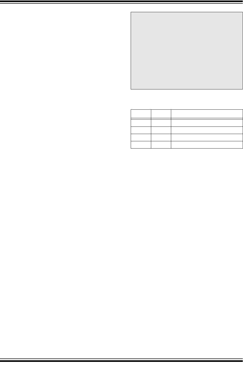
TABLE 18-4: BRG COUNTER
CLOCK RATES
18.1.3.1 ABD and EUSART Transmission
Since the BRG clock is reversed during ABD acquisi-
tion, the EUSART transmitter cannot be used during
ABD. This means that whenever the ABDEN bit is set,
TXREG cannot be written to. Users should also ensure
that ABDEN does not become set during a transmit
sequence. Failing to do this may result in unpredictable
EUSART operation.
Note 1: If the WUE bit is set with the ABDEN bit,
Auto-Baud Rate Detection will occur on
the byte following the Break character.
2: It is up to the user to determine that the
incoming character baud rate is within the
range of the selected BRG clock source.
Some combinations of oscillator frequency
and EUSART baud rates are not possible
due to bit error rates. Overall system
timing and communication baud rates
must be taken into consideration when
using the Auto-Baud Rate Detection
feature.
BRG16 BRGH BRG Counter Clock
00 F
OSC/512
01 FOSC/128
10 FOSC/128
11 F
OSC/32
Note: During the ABD sequence, SPBRG and
SPBRGH are both used as a 16-bit counter,
independent of BRG16 setting.