
Datasheet


Table Of Contents
- Power Management Features:
- Flexible Oscillator Structure:
- Peripheral Highlights:
- Peripheral Highlights (Continued):
- Special Microcontroller Features:
- Pin Diagrams
- Pin Diagrams (Cont.’d)
- Table of Contents
- Most Current Data Sheet
- Errata
- Customer Notification System
- 1.0 Device Overview
- 2.0 Oscillator Configurations
- 3.0 Power-Managed Modes
- 4.0 Reset
- 4.1 RCON Register
- 4.2 Master Clear (MCLR)
- 4.3 Power-on Reset (POR)
- 4.4 Brown-out Reset (BOR)
- 4.5 Device Reset Timers
- 4.5.1 Power-up Timer (PWRT)
- 4.5.2 Oscillator Start-up Timer (OST)
- 4.5.3 PLL Lock Time-out
- 4.5.4 Time-out Sequence
- TABLE 4-2: Time-out in Various Situations
- FIGURE 4-3: Time-out Sequence on Power-up (MCLR Tied to Vdd, Vdd Rise < Tpwrt)
- FIGURE 4-4: Time-out Sequence on Power-up (MCLR Not Tied to Vdd): Case 1
- FIGURE 4-5: Time-out Sequence on Power-up (MCLR Not Tied to Vdd): Case 2
- FIGURE 4-6: Slow Rise Time (MCLR Tied to Vdd, Vdd Rise > Tpwrt)
- FIGURE 4-7: Time-out Sequence on POR w/PLL Enabled (MCLR Tied to Vdd)
- 4.6 Reset State of Registers
- 5.0 Memory Organization
- 5.1 Program Memory Organization
- 5.2 PIC18 Instruction Cycle
- 5.3 Data Memory Organization
- 5.4 Data Addressing Modes
- 5.5 Data Memory and the Extended Instruction Set
- 5.6 PIC18 Instruction Execution and the Extended Instruction Set
- 6.0 Data EEPROM Memory
- 7.0 Flash Program Memory
- 7.1 Table Reads and Table Writes
- 7.2 Control Registers
- 7.3 Reading the Flash Program Memory
- 7.4 Erasing Flash Program Memory
- 7.5 Writing to Flash Program Memory
- 7.6 Flash Program Operation During Code Protection
- 8.0 8 X 8 Hardware Multiplier
- 8.1 Introduction
- 8.2 Operation
- EXAMPLE 8-1: 8 x 8 Unsigned Multiply Routine
- EXAMPLE 8-2: 8 x 8 Signed Multiply Routine
- TABLE 8-1: Performance Comparison for Various Multiply Operations
- EQUATION 8-1: 16 x 16 Unsigned Multiplication Algorithm
- EXAMPLE 8-3: 16 x 16 Unsigned Multiply Routine
- EQUATION 8-2: 16 x 16 Signed Multiplication Algorithm
- EXAMPLE 8-4: 16 x 16 Signed Multiply Routine
- 9.0 I/O Ports
- 10.0 Interrupts
- 11.0 Timer0 Module
- 12.0 Timer1 Module
- 13.0 Timer2 Module
- 14.0 Timer3 Module
- 15.0 Capture/Compare/PWM (CCP) Modules
- Register 15-1: CCPxCON: CCPx Control Register (28-Pin Devices)
- 15.1 CCP Module Configuration
- 15.2 Capture Mode
- 15.3 Compare Mode
- 15.4 PWM Mode
- 16.0 Enhanced Capture/ Compare/PWM (ECCP) Module
- Register 16-1: CCP1CON: ECCP Control Register (40/44-Pin Devices)
- 16.1 ECCP Outputs and Configuration
- 16.2 Capture and Compare Modes
- 16.3 Standard PWM Mode
- 16.4 Enhanced PWM Mode
- 16.4.1 PWM Period
- 16.4.2 PWM Duty Cycle
- 16.4.3 PWM Output Configurations
- 16.4.4 Half-Bridge Mode
- 16.4.5 Full-Bridge Mode
- 16.4.6 Programmable Dead-Band Delay
- 16.4.7 Enhanced PWM Auto-Shutdown
- 16.4.8 Start-up Considerations
- 16.4.9 Setup for PWM Operation
- 16.4.10 Operation in Power-Managed Modes
- 16.4.11 Effects of a Reset
- 17.0 Master Synchronous Serial Port (MSSP) Module
- 17.1 Master SSP (MSSP) Module Overview
- 17.2 Control Registers
- 17.3 SPI Mode
- 17.4 I2C Mode
- FIGURE 17-7: MSSP Block Diagram (I2C™ Mode)
- 17.4.1 Registers
- 17.4.2 Operation
- 17.4.3 Slave Mode
- 17.4.4 Clock Stretching
- 17.4.5 General Call Address Support
- 17.4.6 Master Mode
- 17.4.7 Baud Rate
- 17.4.8 I2C Master Mode Start Condition Timing
- 17.4.9 I2C Master Mode Repeated Start Condition Timing
- 17.4.10 I2C Master Mode Transmission
- 17.4.11 I2C Master Mode Reception
- 17.4.12 Acknowledge Sequence Timing
- 17.4.13 Stop Condition Timing
- 17.4.14 Sleep Operation
- 17.4.15 Effects of a Reset
- 17.4.16 Multi-Master Mode
- 17.4.17 Multi -Master Communication, Bus Collision and Bus Arbitration
- FIGURE 17-25: Bus Collision Timing for Transmit and Acknowledge
- FIGURE 17-26: Bus Collision During Start Condition (SDA Only)
- FIGURE 17-27: Bus Collision During Start Condition (SCL = 0)
- FIGURE 17-28: BRG Reset Due to SDA Arbitration During Start Condition
- FIGURE 17-29: Bus Collision During a Repeated Start Condition (Case 1)
- FIGURE 17-30: Bus Collision During Repeated Start Condition (Case 2)
- FIGURE 17-31: Bus Collision During a Stop Condition (Case 1)
- FIGURE 17-32: Bus Collision During a Stop Condition (Case 2)
- 18.0 Enhanced Universal Synchronous Receiver Transmitter (EUSART)
- Register 18-1: TXSTA: Transmit Status And Control Register
- Register 18-2: RCSTA: Receive Status And Control Register
- Register 18-3: BAUDCON: Baud Rate Control Register
- 18.1 Baud Rate Generator (BRG)
- 18.2 EUSART Asynchronous Mode
- 18.3 EUSART Synchronous Master Mode
- 18.4 EUSART Synchronous Slave Mode
- 19.0 10-Bit Analog-to-Digital Converter (A/D) Module
- Register 19-1: ADCON0: A/D Control Register 0
- Register 19-2: ADCON1: A/D Control Register 1
- Register 19-3: ADCON2: A/D Control Register 2
- FIGURE 19-1: A/D Block Diagram
- FIGURE 19-2: A/D Transfer Function
- FIGURE 19-3: Analog Input Model
- 19.1 A/D Acquisition Requirements
- 19.2 Selecting and Configuring Acquisition Time
- 19.3 Selecting the A/D Conversion Clock
- 19.4 Operation in Power-Managed Modes
- 19.5 Configuring Analog Port Pins
- 19.6 A/D Conversions
- 19.7 Discharge
- 19.8 Use of the CCP2 Trigger
- 20.0 Comparator Module
- Register 20-1: CMCON: Comparator Control Register
- 20.1 Comparator Configuration
- 20.2 Comparator Operation
- 20.3 Comparator Reference
- 20.4 Comparator Response Time
- 20.5 Comparator Outputs
- 20.6 Comparator Interrupts
- 20.7 Comparator Operation During Sleep
- 20.8 Effects of a Reset
- 20.9 Analog Input Connection Considerations
- 21.0 Comparator Voltage Reference Module
- 22.0 High/Low-Voltage Detect (HLVD)
- 23.0 Special Features of the CPU
- 23.1 Configuration Bits
- TABLE 23-1: Configuration Bits and Device IDs
- Register 23-1: CONFIG1h: Configuration Register 1 High (Byte Address 300001h)
- Register 23-2: CONFIG2L: Configuration Register 2 Low (Byte Address 300002h)
- Register 23-3: CONFIG2H: Configuration Register 2 High (Byte Address 300003h)
- Register 23-4: CONFIG3H: Configuration Register 3 High (Byte Address 300005h)
- Register 23-5: CONFIG4L: Configuration Register 4 Low (Byte Address 300006h)
- Register 23-6: CONFIG5L: Configuration Register 5 Low (Byte Address 300008h)
- Register 23-7: CONFIG5H: Configuration Register 5 High (Byte Address 300009h)
- Register 23-8: CONFIG6L: Configuration Register 6 Low (Byte Address 30000Ah)
- Register 23-9: CONFIG6H: Configuration Register 6 High (Byte Address 30000Bh)
- Register 23-10: CONFIG7L: Configuration Register 7 Low (Byte Address 30000Ch)
- Register 23-11: CONFIG7H: Configuration Register 7 High (Byte Address 30000Dh)
- Register 23-12: DEVID1: Device ID Register 1 for PIC18F2525/2620/4525/4620
- Register 23-13: DEVID2: Device ID Register 2 for PIC18F2525/2620/4525/4620
- 23.2 Watchdog Timer (WDT)
- 23.3 Two-Speed Start-up
- 23.4 Fail-Safe Clock Monitor
- 23.5 Program Verification and Code Protection
- 23.6 ID Locations
- 23.7 In-Circuit Serial Programming
- 23.8 In-Circuit Debugger
- 23.9 Single-Supply ICSP Programming
- 23.1 Configuration Bits
- 24.0 Instruction Set Summary
- 24.1 Standard Instruction Set
- 24.2 Extended Instruction Set
- 25.0 Development Support
- 25.1 MPLAB Integrated Development Environment Software
- 25.2 MPASM Assembler
- 25.3 MPLAB C18 and MPLAB C30 C Compilers
- 25.4 MPLINK Object Linker/ MPLIB Object Librarian
- 25.5 MPLAB ASM30 Assembler, Linker and Librarian
- 25.6 MPLAB SIM Software Simulator
- 25.7 MPLAB ICE 2000 High-Performance In-Circuit Emulator
- 25.8 MPLAB REAL ICE In-Circuit Emulator System
- 25.9 MPLAB ICD 2 In-Circuit Debugger
- 25.10 MPLAB PM3 Device Programmer
- 25.11 PICSTART Plus Development Programmer
- 25.12 PICkit 2 Development Programmer
- 25.13 Demonstration, Development and Evaluation Boards
- 26.0 Electrical Characteristics
- Absolute Maximum Ratings(†)
- 26.1 DC Characteristics: Supply Voltage PIC18F2525/2620/4525/4620 (Industrial) PIC18LF2525/2620/4525/4620 (Industrial)
- 26.2 DC Characteristics: Power-Down and Supply Current PIC18F2525/2620/4525/4620 (Industrial) PIC18LF2525/2620/4525/4620 (Industrial)
- 26.3 DC Characteristics: PIC18F2525/2620/4525/4620 (Industrial) PIC18LF2525/2620/4525/4620 (Industrial)
- 26.4 AC (Timing) Characteristics
- 26.4.1 Timing Parameter Symbology
- 26.4.2 Timing Conditions
- 26.4.3 Timing Diagrams and Specifications
- FIGURE 26-6: External Clock Timing (All Modes Except PLL)
- TABLE 26-6: External Clock Timing Requirements
- TABLE 26-7: PLL Clock Timing Specifications (Vdd = 4.2V to 5.5V)
- TABLE 26-8: AC Characteristics: Internal RC Accuracy PIC18F2525/2620/4525/4620 (Industrial) PIC18LF2525/2620/4525/4620 (Industrial)
- FIGURE 26-7: CLKO and I/O Timing
- TABLE 26-9: CLKO and I/O Timing Requirements
- FIGURE 26-8: Reset, Watchdog Timer, Oscillator Start-up Timer and Power-up Timer Timing
- FIGURE 26-9: Brown-out Reset Timing
- TABLE 26-10: Reset, Watchdog Timer, Oscillator Start-up Timer, Power-up Timer and Brown-out Reset Requirements
- FIGURE 26-10: Timer0 and Timer1 External Clock Timings
- TABLE 26-11: Timer0 and Timer1 External Clock Requirements
- FIGURE 26-11: Capture/Compare/PWM Timings (All CCP Modules)
- TABLE 26-12: Capture/Compare/PWM Requirements (All CCP Modules)
- FIGURE 26-12: Parallel Slave Port Timing (PIC18F4525/4620)
- TABLE 26-13: Parallel Slave Port Requirements (PIC18F4525/4620)
- FIGURE 26-13: Example SPI Master Mode Timing (CKE = 0)
- TABLE 26-14: Example SPI Mode Requirements (Master Mode, CKE = 0)
- FIGURE 26-14: Example SPI Master Mode Timing (CKE = 1)
- TABLE 26-15: Example SPI Mode Requirements (Master Mode, CKE = 1)
- FIGURE 26-15: Example Spi Slave Mode Timing (CKE = 0)
- TABLE 26-16: Example SPI Mode Requirements (Slave Mode Timing, CKE = 0)
- FIGURE 26-16: Example SPI Slave Mode Timing (CKE = 1)
- TABLE 26-17: Example SPI Slave Mode Requirements (CKE = 1)
- FIGURE 26-17: I2C™ Bus Start/Stop Bits Timing
- TABLE 26-18: I2C™ Bus Start/Stop Bits Requirements (Slave Mode)
- FIGURE 26-18: I2C™ Bus Data Timing
- TABLE 26-19: I2C™ Bus Data Requirements (Slave Mode)
- FIGURE 26-19: Master SSP I2C™ Bus Start/Stop Bits Timing Waveforms
- TABLE 26-20: Master SSP I2C™ Bus Start/Stop Bits Requirements
- FIGURE 26-20: Master SSP I2C™ Bus Data Timing
- TABLE 26-21: Master SSP I2C™ Bus Data Requirements
- FIGURE 26-21: EUSART Synchronous Transmission (Master/Slave) Timing
- TABLE 26-22: EUSART Synchronous Transmission Requirements
- FIGURE 26-22: EUSART Synchronous Receive (Master/Slave) Timing
- TABLE 26-23: EUSART Synchronous Receive Requirements
- TABLE 26-24: A/D Converter Characteristics: PIC18F2525/2620/4525/4620 (Industrial) PIC18LF2525/2620/4525/4620 (Industrial)
- FIGURE 26-23: A/D Conversion Timing
- TABLE 26-25: A/D Conversion Requirements
- 27.0 DC and AC Characteristics Graphs and Tables
- FIGURE 27-1: Sleep Mode
- FIGURE 27-2: Typical Ipd vs. Vdd Across Temperature (Sleep Mode)
- FIGURE 27-3: Maximum Ipd vs. Vdd Across Temperature (Sleep Mode)
- FIGURE 27-4: Typical T1OSC Delta Current vs. Vdd Across Temp. (Device in Sleep, T1OSC in Low-Power Mode)
- FIGURE 27-5: Maximum T1OSC Delta Current vs. Vdd Across Temp. (Device in Sleep, TIOSC in Low-Power Mode)
- FIGURE 27-6: Typical T1OSC Delta Current vs. Vdd Across Temp. (Device in Sleep, T1OSC in High-Power Mode)
- FIGURE 27-7: Maximum T1OSC Delta Current vs. Vdd Across Temp. (Device in Sleep, T1OSC in High-Power Mode)
- FIGURE 27-8: Typical BOR Delta Current vs. Vdd Across Temp. (BORV = 2.7V, Sleep Mode)
- FIGURE 27-9: Typical WDT Current vs. Vdd Across Temperature (WDT Delta Current in Sleep Mode)
- FIGURE 27-10: Maximum WDT Current vs. Vdd Across Temperature (WDT Delta Current in Sleep Mode)
- FIGURE 27-11: Typical Idd Across Vdd (RC_RUN Mode, 25°C)
- FIGURE 27-12: Maximum Idd Across Vdd (RC_RUN Mode, 85°C)
- FIGURE 27-13: Typical and Maximum Idd Across Vdd (RC_RUN Mode, 31 kHz)
- FIGURE 27-14: Typical Idd Across Vdd (RC_IDLE Mode, 25°C)
- FIGURE 27-15: Maximum Idd Across Vdd (RC_IDLE Mode, -40°C-85°C)
- FIGURE 27-16: Typical and Maximum Idd Across Vdd (RC_IDLE Mode, 31 kHz)
- FIGURE 27-17: Typical and Maximum SEC_RUN Current vs. Vdd Across Temperature (T1OSC in Low-Power Mode)
- FIGURE 27-18: Typical and Maximum SEC_IDLE Current vs. Vdd Across Temperature (T1OSC in Low-Power Mode)
- FIGURE 27-19: Typical Idd vs. Fosc, 500 kHz to 4 MHz (PRI_RUN Mode (EC Clock), 25°C)
- FIGURE 27-20: Maximum Idd vs. Fosc, 500 kHz to 4 MHz (PRI_RUN Mode (EC Clock), -40°C to +125°C)
- FIGURE 27-21: Typical Idd vs. Fosc, 4 MHz to 40 MHz (PRI_RUN Mode (EC Clock), 25°C)
- FIGURE 27-22: Maximum Idd vs. Fosc, 4 MHz to 40 MHz (PRI_RUN Mode (EC Clock), -40°C to +125°C)
- FIGURE 27-23: Typical Idd vs. Fosc, HS/PLL (PRI_RUN Mode, 25°C)
- FIGURE 27-24: Maximum Idd vs. Fosc, HS/PLL (PRI_RUN Mode, -40°C)
- FIGURE 27-25: Typical Idd vs. Fosc, 500 kHz to 4 MHz (PRI_IDLE Mode, 25°C)
- FIGURE 27-26: Maximum Idd vs. Fosc, 500 kHz to 4 MHz (PRI_IDLE Mode, -40°C to +125°C)
- FIGURE 27-27: Typical Idd vs. Fosc, 4 MHz to 40 MHz (PRI_IDLE Mode, 25°C)
- FIGURE 27-28: Maximum Idd vs. Fosc, 4 MHz to 40 MHz (PRI_IDLE Mode, -40°C to +125°C)
- FIGURE 27-29: Typical Idd vs. Fosc, HS/PLL (PRI_IDLE Mode, 25°C)
- FIGURE 27-30: Maximum Idd vs. Fosc, HS/PLL (PRI_IDLE Mode, -40°C)
- FIGURE 27-31: Vin (ST) vs. Vdd, 25°C (-40°C to +125°C)
- FIGURE 27-32: Vin (TTL) vs. Vdd, 25°C (-40°C to +125°C)
- FIGURE 27-33: Vol vs. Iol (Vdd = 3.0V, -40°C to +85°C)
- FIGURE 27-34: Vol vs. Iol (Vdd = 5.0V, -40°C to +125°C)
- FIGURE 27-35: Voh vs. Ioh (Vdd = 3.0V, -40°C to +85°C)
- FIGURE 27-36: Voh vs. Ioh (Vdd = 5.0V, -40°C to +125°C)
- FIGURE 27-37: INTOSC Frequency vs. Vdd, Temperature (-40°C, +25°C, +85°C, +125°C)
- FIGURE 27-38: INTRC vs. Vdd Across Temperature (-40°C to +125°C)
- FIGURE 27-39: WDT Period vs. Vdd Across Temperature (1:1 Postscaler, -40°C to +125°C)
- 28.0 Packaging Information
- Appendix A: Revision History
- Appendix B: Device Differences
- Appendix C: Conversion Considerations
- Appendix D: Migration from Baseline to Enhanced Devices
- Appendix E: Migration from Mid-Range TO Enhanced Devices
- Appendix F: Migration from High-End to Enhanced Devices
- INDEX
- Worldwide Sales and Service
© 2008 Microchip Technology Inc. DS39626E-page 43
PIC18F2525/2620/4525/4620
4.2 Master Clear (MCLR)
The MCLR pin provides a method for triggering an
external Reset of the device. A Reset is generated by
holding the pin low. These devices have a noise filter in
the MCLR
Reset path which detects and ignores small
pulses.
The MCLR
pin is not driven low by any internal Resets,
including the WDT.
In PIC18F2525/2620/4525/4620 devices, the MCLR
input can be disabled with the MCLRE Configuration
bit. When MCLR
is disabled, the pin becomes a digital
input. See Section 9.5 “PORTE, TRISE and LATE
Registers” for more information.
4.3 Power-on Reset (POR)
A Power-on Reset pulse is generated on-chip
whenever V
DD rises above a certain threshold. This
allows the device to start in the initialized state when
VDD is adequate for operation.
To take advantage of the POR circuitry, tie the MCLR
pin through a resistor (1 kΩ to 10 kΩ) to VDD. This will
eliminate external RC components usually needed to
create a Power-on Reset delay. A minimum rise rate for
V
DD is specified (parameter D004). For a slow rise
time, see Figure 4-2.
When the device starts normal operation (i.e., exits the
Reset condition), device operating parameters
(voltage, frequency, temperature, etc.) must be met to
ensure operation. If these conditions are not met, the
device must be held in Reset until the operating
conditions are met.
POR events are captured by the POR
bit (RCON<1>).
The state of the bit is set to ‘0’ whenever a POR occurs;
it does not change for any other Reset event. POR is
not reset to ‘1’ by any hardware event. To capture
multiple events, the user manually resets the bit to ‘1’
in software following any POR.
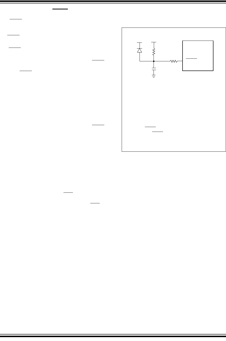
FIGURE 4-2: EXTERNAL POWER-ON
RESET CIRCUIT (FOR
SLOW V
DD POWER-UP)
Note 1: External Power-on Reset circuit is required
only if the V
DD power-up slope is too slow.
The diode D helps discharge the capacitor
quickly when V
DD powers down.
2: R < 40 kΩ is recommended to make sure that
the voltage drop across R does not violate
the device’s electrical specification.
3: R1 ≥ 1 kΩ will limit any current flowing into
MCLR
from external capacitor C, in the event
of MCLR
/VPP pin breakdown, due to
Electrostatic Discharge (ESD) or Electrical
Overstress (EOS).
C
R1
R
D
V
DD
MCLR
PIC18FXXXX
VDD