
Datasheet


Table Of Contents
- Power Management Features:
- Flexible Oscillator Structure:
- Peripheral Highlights:
- Peripheral Highlights (Continued):
- Special Microcontroller Features:
- Pin Diagrams
- Pin Diagrams (Cont.’d)
- Table of Contents
- Most Current Data Sheet
- Errata
- Customer Notification System
- 1.0 Device Overview
- 2.0 Oscillator Configurations
- 3.0 Power-Managed Modes
- 4.0 Reset
- 4.1 RCON Register
- 4.2 Master Clear (MCLR)
- 4.3 Power-on Reset (POR)
- 4.4 Brown-out Reset (BOR)
- 4.5 Device Reset Timers
- 4.5.1 Power-up Timer (PWRT)
- 4.5.2 Oscillator Start-up Timer (OST)
- 4.5.3 PLL Lock Time-out
- 4.5.4 Time-out Sequence
- TABLE 4-2: Time-out in Various Situations
- FIGURE 4-3: Time-out Sequence on Power-up (MCLR Tied to Vdd, Vdd Rise < Tpwrt)
- FIGURE 4-4: Time-out Sequence on Power-up (MCLR Not Tied to Vdd): Case 1
- FIGURE 4-5: Time-out Sequence on Power-up (MCLR Not Tied to Vdd): Case 2
- FIGURE 4-6: Slow Rise Time (MCLR Tied to Vdd, Vdd Rise > Tpwrt)
- FIGURE 4-7: Time-out Sequence on POR w/PLL Enabled (MCLR Tied to Vdd)
- 4.6 Reset State of Registers
- 5.0 Memory Organization
- 5.1 Program Memory Organization
- 5.2 PIC18 Instruction Cycle
- 5.3 Data Memory Organization
- 5.4 Data Addressing Modes
- 5.5 Data Memory and the Extended Instruction Set
- 5.6 PIC18 Instruction Execution and the Extended Instruction Set
- 6.0 Data EEPROM Memory
- 7.0 Flash Program Memory
- 7.1 Table Reads and Table Writes
- 7.2 Control Registers
- 7.3 Reading the Flash Program Memory
- 7.4 Erasing Flash Program Memory
- 7.5 Writing to Flash Program Memory
- 7.6 Flash Program Operation During Code Protection
- 8.0 8 X 8 Hardware Multiplier
- 8.1 Introduction
- 8.2 Operation
- EXAMPLE 8-1: 8 x 8 Unsigned Multiply Routine
- EXAMPLE 8-2: 8 x 8 Signed Multiply Routine
- TABLE 8-1: Performance Comparison for Various Multiply Operations
- EQUATION 8-1: 16 x 16 Unsigned Multiplication Algorithm
- EXAMPLE 8-3: 16 x 16 Unsigned Multiply Routine
- EQUATION 8-2: 16 x 16 Signed Multiplication Algorithm
- EXAMPLE 8-4: 16 x 16 Signed Multiply Routine
- 9.0 I/O Ports
- 10.0 Interrupts
- 11.0 Timer0 Module
- 12.0 Timer1 Module
- 13.0 Timer2 Module
- 14.0 Timer3 Module
- 15.0 Capture/Compare/PWM (CCP) Modules
- Register 15-1: CCPxCON: CCPx Control Register (28-Pin Devices)
- 15.1 CCP Module Configuration
- 15.2 Capture Mode
- 15.3 Compare Mode
- 15.4 PWM Mode
- 16.0 Enhanced Capture/ Compare/PWM (ECCP) Module
- Register 16-1: CCP1CON: ECCP Control Register (40/44-Pin Devices)
- 16.1 ECCP Outputs and Configuration
- 16.2 Capture and Compare Modes
- 16.3 Standard PWM Mode
- 16.4 Enhanced PWM Mode
- 16.4.1 PWM Period
- 16.4.2 PWM Duty Cycle
- 16.4.3 PWM Output Configurations
- 16.4.4 Half-Bridge Mode
- 16.4.5 Full-Bridge Mode
- 16.4.6 Programmable Dead-Band Delay
- 16.4.7 Enhanced PWM Auto-Shutdown
- 16.4.8 Start-up Considerations
- 16.4.9 Setup for PWM Operation
- 16.4.10 Operation in Power-Managed Modes
- 16.4.11 Effects of a Reset
- 17.0 Master Synchronous Serial Port (MSSP) Module
- 17.1 Master SSP (MSSP) Module Overview
- 17.2 Control Registers
- 17.3 SPI Mode
- 17.4 I2C Mode
- FIGURE 17-7: MSSP Block Diagram (I2C™ Mode)
- 17.4.1 Registers
- 17.4.2 Operation
- 17.4.3 Slave Mode
- 17.4.4 Clock Stretching
- 17.4.5 General Call Address Support
- 17.4.6 Master Mode
- 17.4.7 Baud Rate
- 17.4.8 I2C Master Mode Start Condition Timing
- 17.4.9 I2C Master Mode Repeated Start Condition Timing
- 17.4.10 I2C Master Mode Transmission
- 17.4.11 I2C Master Mode Reception
- 17.4.12 Acknowledge Sequence Timing
- 17.4.13 Stop Condition Timing
- 17.4.14 Sleep Operation
- 17.4.15 Effects of a Reset
- 17.4.16 Multi-Master Mode
- 17.4.17 Multi -Master Communication, Bus Collision and Bus Arbitration
- FIGURE 17-25: Bus Collision Timing for Transmit and Acknowledge
- FIGURE 17-26: Bus Collision During Start Condition (SDA Only)
- FIGURE 17-27: Bus Collision During Start Condition (SCL = 0)
- FIGURE 17-28: BRG Reset Due to SDA Arbitration During Start Condition
- FIGURE 17-29: Bus Collision During a Repeated Start Condition (Case 1)
- FIGURE 17-30: Bus Collision During Repeated Start Condition (Case 2)
- FIGURE 17-31: Bus Collision During a Stop Condition (Case 1)
- FIGURE 17-32: Bus Collision During a Stop Condition (Case 2)
- 18.0 Enhanced Universal Synchronous Receiver Transmitter (EUSART)
- Register 18-1: TXSTA: Transmit Status And Control Register
- Register 18-2: RCSTA: Receive Status And Control Register
- Register 18-3: BAUDCON: Baud Rate Control Register
- 18.1 Baud Rate Generator (BRG)
- 18.2 EUSART Asynchronous Mode
- 18.3 EUSART Synchronous Master Mode
- 18.4 EUSART Synchronous Slave Mode
- 19.0 10-Bit Analog-to-Digital Converter (A/D) Module
- Register 19-1: ADCON0: A/D Control Register 0
- Register 19-2: ADCON1: A/D Control Register 1
- Register 19-3: ADCON2: A/D Control Register 2
- FIGURE 19-1: A/D Block Diagram
- FIGURE 19-2: A/D Transfer Function
- FIGURE 19-3: Analog Input Model
- 19.1 A/D Acquisition Requirements
- 19.2 Selecting and Configuring Acquisition Time
- 19.3 Selecting the A/D Conversion Clock
- 19.4 Operation in Power-Managed Modes
- 19.5 Configuring Analog Port Pins
- 19.6 A/D Conversions
- 19.7 Discharge
- 19.8 Use of the CCP2 Trigger
- 20.0 Comparator Module
- Register 20-1: CMCON: Comparator Control Register
- 20.1 Comparator Configuration
- 20.2 Comparator Operation
- 20.3 Comparator Reference
- 20.4 Comparator Response Time
- 20.5 Comparator Outputs
- 20.6 Comparator Interrupts
- 20.7 Comparator Operation During Sleep
- 20.8 Effects of a Reset
- 20.9 Analog Input Connection Considerations
- 21.0 Comparator Voltage Reference Module
- 22.0 High/Low-Voltage Detect (HLVD)
- 23.0 Special Features of the CPU
- 23.1 Configuration Bits
- TABLE 23-1: Configuration Bits and Device IDs
- Register 23-1: CONFIG1h: Configuration Register 1 High (Byte Address 300001h)
- Register 23-2: CONFIG2L: Configuration Register 2 Low (Byte Address 300002h)
- Register 23-3: CONFIG2H: Configuration Register 2 High (Byte Address 300003h)
- Register 23-4: CONFIG3H: Configuration Register 3 High (Byte Address 300005h)
- Register 23-5: CONFIG4L: Configuration Register 4 Low (Byte Address 300006h)
- Register 23-6: CONFIG5L: Configuration Register 5 Low (Byte Address 300008h)
- Register 23-7: CONFIG5H: Configuration Register 5 High (Byte Address 300009h)
- Register 23-8: CONFIG6L: Configuration Register 6 Low (Byte Address 30000Ah)
- Register 23-9: CONFIG6H: Configuration Register 6 High (Byte Address 30000Bh)
- Register 23-10: CONFIG7L: Configuration Register 7 Low (Byte Address 30000Ch)
- Register 23-11: CONFIG7H: Configuration Register 7 High (Byte Address 30000Dh)
- Register 23-12: DEVID1: Device ID Register 1 for PIC18F2525/2620/4525/4620
- Register 23-13: DEVID2: Device ID Register 2 for PIC18F2525/2620/4525/4620
- 23.2 Watchdog Timer (WDT)
- 23.3 Two-Speed Start-up
- 23.4 Fail-Safe Clock Monitor
- 23.5 Program Verification and Code Protection
- 23.6 ID Locations
- 23.7 In-Circuit Serial Programming
- 23.8 In-Circuit Debugger
- 23.9 Single-Supply ICSP Programming
- 23.1 Configuration Bits
- 24.0 Instruction Set Summary
- 24.1 Standard Instruction Set
- 24.2 Extended Instruction Set
- 25.0 Development Support
- 25.1 MPLAB Integrated Development Environment Software
- 25.2 MPASM Assembler
- 25.3 MPLAB C18 and MPLAB C30 C Compilers
- 25.4 MPLINK Object Linker/ MPLIB Object Librarian
- 25.5 MPLAB ASM30 Assembler, Linker and Librarian
- 25.6 MPLAB SIM Software Simulator
- 25.7 MPLAB ICE 2000 High-Performance In-Circuit Emulator
- 25.8 MPLAB REAL ICE In-Circuit Emulator System
- 25.9 MPLAB ICD 2 In-Circuit Debugger
- 25.10 MPLAB PM3 Device Programmer
- 25.11 PICSTART Plus Development Programmer
- 25.12 PICkit 2 Development Programmer
- 25.13 Demonstration, Development and Evaluation Boards
- 26.0 Electrical Characteristics
- Absolute Maximum Ratings(†)
- 26.1 DC Characteristics: Supply Voltage PIC18F2525/2620/4525/4620 (Industrial) PIC18LF2525/2620/4525/4620 (Industrial)
- 26.2 DC Characteristics: Power-Down and Supply Current PIC18F2525/2620/4525/4620 (Industrial) PIC18LF2525/2620/4525/4620 (Industrial)
- 26.3 DC Characteristics: PIC18F2525/2620/4525/4620 (Industrial) PIC18LF2525/2620/4525/4620 (Industrial)
- 26.4 AC (Timing) Characteristics
- 26.4.1 Timing Parameter Symbology
- 26.4.2 Timing Conditions
- 26.4.3 Timing Diagrams and Specifications
- FIGURE 26-6: External Clock Timing (All Modes Except PLL)
- TABLE 26-6: External Clock Timing Requirements
- TABLE 26-7: PLL Clock Timing Specifications (Vdd = 4.2V to 5.5V)
- TABLE 26-8: AC Characteristics: Internal RC Accuracy PIC18F2525/2620/4525/4620 (Industrial) PIC18LF2525/2620/4525/4620 (Industrial)
- FIGURE 26-7: CLKO and I/O Timing
- TABLE 26-9: CLKO and I/O Timing Requirements
- FIGURE 26-8: Reset, Watchdog Timer, Oscillator Start-up Timer and Power-up Timer Timing
- FIGURE 26-9: Brown-out Reset Timing
- TABLE 26-10: Reset, Watchdog Timer, Oscillator Start-up Timer, Power-up Timer and Brown-out Reset Requirements
- FIGURE 26-10: Timer0 and Timer1 External Clock Timings
- TABLE 26-11: Timer0 and Timer1 External Clock Requirements
- FIGURE 26-11: Capture/Compare/PWM Timings (All CCP Modules)
- TABLE 26-12: Capture/Compare/PWM Requirements (All CCP Modules)
- FIGURE 26-12: Parallel Slave Port Timing (PIC18F4525/4620)
- TABLE 26-13: Parallel Slave Port Requirements (PIC18F4525/4620)
- FIGURE 26-13: Example SPI Master Mode Timing (CKE = 0)
- TABLE 26-14: Example SPI Mode Requirements (Master Mode, CKE = 0)
- FIGURE 26-14: Example SPI Master Mode Timing (CKE = 1)
- TABLE 26-15: Example SPI Mode Requirements (Master Mode, CKE = 1)
- FIGURE 26-15: Example Spi Slave Mode Timing (CKE = 0)
- TABLE 26-16: Example SPI Mode Requirements (Slave Mode Timing, CKE = 0)
- FIGURE 26-16: Example SPI Slave Mode Timing (CKE = 1)
- TABLE 26-17: Example SPI Slave Mode Requirements (CKE = 1)
- FIGURE 26-17: I2C™ Bus Start/Stop Bits Timing
- TABLE 26-18: I2C™ Bus Start/Stop Bits Requirements (Slave Mode)
- FIGURE 26-18: I2C™ Bus Data Timing
- TABLE 26-19: I2C™ Bus Data Requirements (Slave Mode)
- FIGURE 26-19: Master SSP I2C™ Bus Start/Stop Bits Timing Waveforms
- TABLE 26-20: Master SSP I2C™ Bus Start/Stop Bits Requirements
- FIGURE 26-20: Master SSP I2C™ Bus Data Timing
- TABLE 26-21: Master SSP I2C™ Bus Data Requirements
- FIGURE 26-21: EUSART Synchronous Transmission (Master/Slave) Timing
- TABLE 26-22: EUSART Synchronous Transmission Requirements
- FIGURE 26-22: EUSART Synchronous Receive (Master/Slave) Timing
- TABLE 26-23: EUSART Synchronous Receive Requirements
- TABLE 26-24: A/D Converter Characteristics: PIC18F2525/2620/4525/4620 (Industrial) PIC18LF2525/2620/4525/4620 (Industrial)
- FIGURE 26-23: A/D Conversion Timing
- TABLE 26-25: A/D Conversion Requirements
- 27.0 DC and AC Characteristics Graphs and Tables
- FIGURE 27-1: Sleep Mode
- FIGURE 27-2: Typical Ipd vs. Vdd Across Temperature (Sleep Mode)
- FIGURE 27-3: Maximum Ipd vs. Vdd Across Temperature (Sleep Mode)
- FIGURE 27-4: Typical T1OSC Delta Current vs. Vdd Across Temp. (Device in Sleep, T1OSC in Low-Power Mode)
- FIGURE 27-5: Maximum T1OSC Delta Current vs. Vdd Across Temp. (Device in Sleep, TIOSC in Low-Power Mode)
- FIGURE 27-6: Typical T1OSC Delta Current vs. Vdd Across Temp. (Device in Sleep, T1OSC in High-Power Mode)
- FIGURE 27-7: Maximum T1OSC Delta Current vs. Vdd Across Temp. (Device in Sleep, T1OSC in High-Power Mode)
- FIGURE 27-8: Typical BOR Delta Current vs. Vdd Across Temp. (BORV = 2.7V, Sleep Mode)
- FIGURE 27-9: Typical WDT Current vs. Vdd Across Temperature (WDT Delta Current in Sleep Mode)
- FIGURE 27-10: Maximum WDT Current vs. Vdd Across Temperature (WDT Delta Current in Sleep Mode)
- FIGURE 27-11: Typical Idd Across Vdd (RC_RUN Mode, 25°C)
- FIGURE 27-12: Maximum Idd Across Vdd (RC_RUN Mode, 85°C)
- FIGURE 27-13: Typical and Maximum Idd Across Vdd (RC_RUN Mode, 31 kHz)
- FIGURE 27-14: Typical Idd Across Vdd (RC_IDLE Mode, 25°C)
- FIGURE 27-15: Maximum Idd Across Vdd (RC_IDLE Mode, -40°C-85°C)
- FIGURE 27-16: Typical and Maximum Idd Across Vdd (RC_IDLE Mode, 31 kHz)
- FIGURE 27-17: Typical and Maximum SEC_RUN Current vs. Vdd Across Temperature (T1OSC in Low-Power Mode)
- FIGURE 27-18: Typical and Maximum SEC_IDLE Current vs. Vdd Across Temperature (T1OSC in Low-Power Mode)
- FIGURE 27-19: Typical Idd vs. Fosc, 500 kHz to 4 MHz (PRI_RUN Mode (EC Clock), 25°C)
- FIGURE 27-20: Maximum Idd vs. Fosc, 500 kHz to 4 MHz (PRI_RUN Mode (EC Clock), -40°C to +125°C)
- FIGURE 27-21: Typical Idd vs. Fosc, 4 MHz to 40 MHz (PRI_RUN Mode (EC Clock), 25°C)
- FIGURE 27-22: Maximum Idd vs. Fosc, 4 MHz to 40 MHz (PRI_RUN Mode (EC Clock), -40°C to +125°C)
- FIGURE 27-23: Typical Idd vs. Fosc, HS/PLL (PRI_RUN Mode, 25°C)
- FIGURE 27-24: Maximum Idd vs. Fosc, HS/PLL (PRI_RUN Mode, -40°C)
- FIGURE 27-25: Typical Idd vs. Fosc, 500 kHz to 4 MHz (PRI_IDLE Mode, 25°C)
- FIGURE 27-26: Maximum Idd vs. Fosc, 500 kHz to 4 MHz (PRI_IDLE Mode, -40°C to +125°C)
- FIGURE 27-27: Typical Idd vs. Fosc, 4 MHz to 40 MHz (PRI_IDLE Mode, 25°C)
- FIGURE 27-28: Maximum Idd vs. Fosc, 4 MHz to 40 MHz (PRI_IDLE Mode, -40°C to +125°C)
- FIGURE 27-29: Typical Idd vs. Fosc, HS/PLL (PRI_IDLE Mode, 25°C)
- FIGURE 27-30: Maximum Idd vs. Fosc, HS/PLL (PRI_IDLE Mode, -40°C)
- FIGURE 27-31: Vin (ST) vs. Vdd, 25°C (-40°C to +125°C)
- FIGURE 27-32: Vin (TTL) vs. Vdd, 25°C (-40°C to +125°C)
- FIGURE 27-33: Vol vs. Iol (Vdd = 3.0V, -40°C to +85°C)
- FIGURE 27-34: Vol vs. Iol (Vdd = 5.0V, -40°C to +125°C)
- FIGURE 27-35: Voh vs. Ioh (Vdd = 3.0V, -40°C to +85°C)
- FIGURE 27-36: Voh vs. Ioh (Vdd = 5.0V, -40°C to +125°C)
- FIGURE 27-37: INTOSC Frequency vs. Vdd, Temperature (-40°C, +25°C, +85°C, +125°C)
- FIGURE 27-38: INTRC vs. Vdd Across Temperature (-40°C to +125°C)
- FIGURE 27-39: WDT Period vs. Vdd Across Temperature (1:1 Postscaler, -40°C to +125°C)
- 28.0 Packaging Information
- Appendix A: Revision History
- Appendix B: Device Differences
- Appendix C: Conversion Considerations
- Appendix D: Migration from Baseline to Enhanced Devices
- Appendix E: Migration from Mid-Range TO Enhanced Devices
- Appendix F: Migration from High-End to Enhanced Devices
- INDEX
- Worldwide Sales and Service
PIC18F2525/2620/4525/4620
DS39626E-page 232 © 2008 Microchip Technology Inc.
19.8 Use of the CCP2 Trigger
An A/D conversion can be started by the Special Event
Trigger of the CCP2 module. This requires that the
CCP2M3:CCP2M0 bits (CCP2CON<3:0>) be
programmed as ‘1011’ and that the A/D module is
enabled (ADON bit is set). When the trigger occurs, the
GO/DONE
bit will be set, starting the A/D acquisition
and conversion and the Timer1 (or Timer3) counter will
be reset to zero. Timer1 (or Timer3) is reset to automat-
ically repeat the A/D acquisition period with minimal
software overhead (moving ADRESH:ADRESL to the
desired location). The appropriate analog input
channel must be selected and the minimum acquisition
period is either timed by the user, or an appropriate
T
ACQ time selected before the Special Event Trigger
sets the GO/DONE
bit (starts a conversion).
If the A/D module is not enabled (ADON is cleared), the
Special Event Trigger will be ignored by the A/D module
but will still reset the Timer1 (or Timer3) counter.
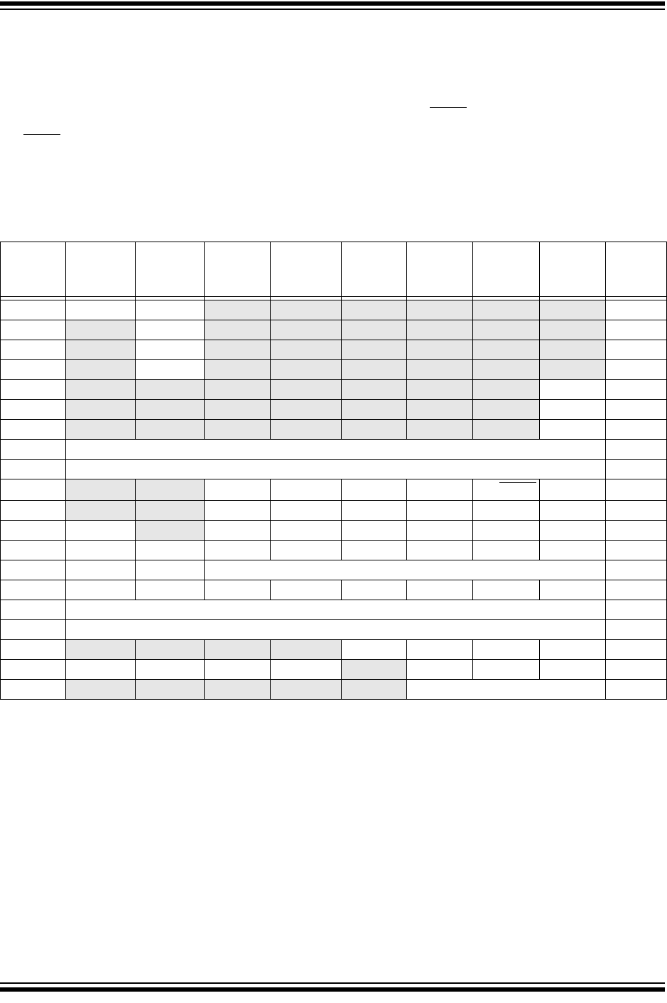
TABLE 19-2: REGISTERS ASSOCIATED WITH A/D OPERATION
Name Bit 7 Bit 6 Bit 5 Bit 4 Bit 3 Bit 2 Bit 1 Bit 0
Reset
Values
on page
INTCON GIE/GIEH PEIE/GIEL
TMR0IE INT0IE RBIE TMR0IF INT0IF RBIF 49
PIR1 PSPIF
(1)
ADIF RCIF TXIF SSPIF CCP1IF TMR2IF TMR1IF 52
PIE1
PSPIE
(1)
ADIE RCIE TXIE SSPIE CCP1IE TMR2IE TMR1IE 52
IPR1 PSPIP
(1)
ADIP RCIP TXIP SSPIP CCP1IP TMR2IP TMR1IP 52
PIR2 OSCFIF CMIF — EEIF BCLIF HLVDIF TMR3IF CCP2IF 52
PIE2
OSCFIE CMIE — EEIE BCLIE HLVDIE TMR3IE CCP2IE 52
IPR2 OSCFIP CMIP — EEIP BCLIP HLVDIP TMR3IP CCP2IP 52
ADRESH A/D Result Register High Byte 51
ADRESL A/D Result Register Low Byte 51
ADCON0
— — CHS3 CHS2 CHS1 CHS0 GO/DONE ADON 51
ADCON1 — — VCFG1 VCFG0 PCFG3 PCFG2 PCFG1 PCFG0 51
ADCON2 ADFM — ACQT2 ACQT1 ACQT0 ADCS2 ADCS1 ADCS0 51
PORTA RA7
(1)
RA6
(1)
RA5 RA4 RA3 RA2 RA1 RA0 52
TRISA TRISA7
(2)
TRISA6
(2)
PORTA Data Direction Control Register 52
PORTB RB7 RB6 RB5 RB4 RB3 RB2 RB1 RB0 52
TRISB PORTB Data Direction Control Register 52
LATB PORTB Data Latch Register (Read and Write to Data Latch) 52
PORTE
(4)
— — — —RE3
(3)
RE2 RE1 RE0 52
TRISE
(4)
IBF OBF IBOV PSPMODE — TRISE2 TRISE1 TRISE0 52
LATE
(4)
— — — — — PORTE Data Latch Register 52
Legend: — = unimplemented, read as ‘0’. Shaded cells are not used for A/D conversion.
Note 1: These bits are unimplemented on 28-pin devices; always maintain these bits clear.
2: PORTA<7:6> and their direction bits are individually configured as port pins based on various primary
oscillator modes. When disabled, these bits read as ‘0’.
3: RE3 port bit is available only as an input pin when the MCLRE Configuration bit is ‘0’.
4: These registers are not implemented on 28-pin devices.