
Datasheet


PIC18(L)F2X/4XK22
DS41412F-page 454 2010-2012 Microchip Technology Inc.
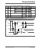
FIGURE 27-12: CAPTURE/COMPARE/PWM TIMINGS (ALL CCP MODULES)
TABLE 27-12: TIMER0 AND TIMER1/3/5 EXTERNAL CLOCK REQUIREMENTS
Param.
No.
Symbol Characteristic Min Max Units Conditions
40 Tt0H
T0CKI High Pulse Width No prescaler 0.5 T
CY + 20 — ns
With prescaler 10 — ns
41 Tt0L
T0CKI Low Pulse Width No prescaler 0.5 T
CY + 20 — ns
With prescaler 10 — ns
42 Tt0P
T0CKI Period No prescaler T
CY + 10 — ns
With prescaler Greater of:
20 ns or
(T
CY + 40)/N
— ns N = prescale
value
(1, 2, 4,..., 256)
45 Tt1H
TxCKI High
Time
Synchronous, no prescaler 0.5 T
CY + 20 — ns
Synchronous,
with prescaler
10 — ns
Asynchronous 30 — ns
46 Tt1L
TxCKI Low
Time
Synchronous, no prescaler 0.5 T
CY + 5 — ns
Synchronous,
with prescaler
10 — ns
Asynchronous 30 — ns
47 Tt1P
TxCKI Input
Period
Synchronous Greater of:
20 ns or
(T
CY + 40)/N
— ns N = prescale
value (1, 2, 4, 8)
Asynchronous 60 — ns
Ft1
TxCKI Clock Input Frequency Range DC 50 kHz
48 Tcke2tmrI
Delay from External TxCKI Clock Edge to Timer
Increment
2 T
OSC 7 TOSC —
Note: Refer to Figure 27-6 for load conditions.
CCPx
(Capture Mode)
50 51
52
CCPx
53
54
(Compare or PWM Mode)