
Datasheet


PIC18(L)F2X/4XK22
DS41412F-page 344 2010-2012 Microchip Technology Inc.
21.3 Register Definitions: FVR Control
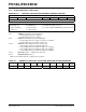
REGISTER 21-1: VREFCON0: FIXED VOLTAGE REFERENCE CONTROL REGISTER
R/W-0 R/W-0 R/W-0 R/W-1 U-0 U-0 U-0 U-0
FVREN FVRST FVRS<1:0>
— — — —
bit 7 bit 0
Legend:
R = Readable bit W = Writable bit U = Unimplemented bit, read as ‘0’
u = Bit is unchanged x = Bit is unknown -n/n = Value at POR and BOR/Value at all other Resets
‘1’ = Bit is set ‘0’ = Bit is cleared
bit 7 FVREN: Fixed Voltage Reference Enable bit
0 = Fixed Voltage Reference is disabled
1 = Fixed Voltage Reference is enabled
bit 6 FVRST: Fixed Voltage Reference Ready Flag bit
0 = Fixed Voltage Reference output is not ready or not enabled
1 = Fixed Voltage Reference output is ready for use
bit 5-4 FVRS<1:0>: Fixed Voltage Reference Selection bits
00 = Fixed Voltage Reference Peripheral output is off
01 = Fixed Voltage Reference Peripheral output is 1x (1.024V)
10 = Fixed Voltage Reference Peripheral output is 2x (2.048V)
(1)
11 = Fixed Voltage Reference Peripheral output is 4x (4.096V)
(1)
bit 3-2 Reserved: Read as ‘0’. Maintain these bits clear.
bit 1-0 Unimplemented: Read as ‘0’.
Note 1: Fixed Voltage Reference output cannot exceed V
DD.
TABLE 21-1: SUMMARY OF REGISTERS ASSOCIATED WITH FIXED VOLTAGE REFERENCE
Name Bit 7 Bit 6 Bit 5 Bit 4 Bit 3 Bit 2 Bit 1 Bit 0
Register
on Page
VREFCON0 FVREN FVRST FVRS<1:0>
— — — —
344
Legend:
— = unimplemented locations, read as ‘0’. Shaded bits are not used by the FVR module.