
Datasheet


2010 Microchip Technology Inc. DS41303G-page 81
PIC18F2XK20/4XK20
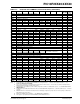
SPBRGH EUSART Baud Rate Generator Register, High Byte 0000 0000 61, 241
SPBRG EUSART Baud Rate Generator Register, Low Byte 0000 0000 61, 241
RCREG EUSART Receive Register 0000 0000 61, 238
TXREG EUSART Transmit Register 0000 0000 61, 237
TXSTA CSRC TX9 TXEN SYNC SENDB BRGH TRMT TX9D 0000 0010 61, 246
RCSTA SPEN RX9 SREN CREN ADDEN FERR OERR RX9D 0000 000x 61, 247
EEADR EEADR7 EEADR6 EEADR5 EEADR4 EEADR3 EEADR2 EEADR1 EEADR0 0000 0000 61, 90, 99
EEADRH
(7)
— — — — — — EEADR9 EEADR8 ---- --00 61, 90, 99
EEDATA EEPROM Data Register 0000 0000 61, 90, 99
EECON2 EEPROM Control Register 2 (not a physical register) 0000 0000 61, 90, 99
EECON1 EEPGD CFGS
— FREE WRERR WREN WR RD xx-0 x000 61, 91, 99
IPR2 OSCFIP C1IP C2IP EEIP BCLIP HLVDIP TMR3IP CCP2IP 1111 1111 62, 117
PIR2 OSCFIF C1IF C2IF EEIF BCLIF HLVDIF TMR3IF CCP2IF 0000 0000 62, 113
PIE2 OSCFIE C1IE C2IE EEIE BCLIE HLVDIE TMR3IE CCP2IE 0000 0000 62, 115
IPR1 PSPIP
(2)
ADIP RCIP TXIP SSPIP CCP1IP TMR2IP TMR1IP 1111 1111 62, 116
PIR1 PSPIF
(2)
ADIF RCIF TXIF SSPIF CCP1IF TMR2IF TMR1IF 0000 0000 62, 112
PIE1 PSPIE
(2)
ADIE RCIE TXIE SSPIE CCP1IE TMR2IE TMR1IE 0000 0000 62, 114
OSCTUNE INTSRC PLLEN
(3)
TUN5 TUN4 TUN3 TUN2 TUN1 TUN0 0q00 0000 33, 62
TRISE
(2)
IBF OBF IBOV PSPMODE — TRISE2 TRISE1 TRISE0 0000 -111 62, 134
TRISD
(2)
PORTD Data Direction Control Register 1111 1111 62, 130
TRISC PORTC Data Direction Control Register 1111 1111 62, 127
TRISB PORTB Data Direction Control Register 1111 1111 62, 124
TRISA TRISA7
(5)
TRISA6
(5)
Data Direction Control Register for PORTA 1111 1111 62, 121
LATE
(2)
— — — — — PORTE Data Latch Register
(Read and Write to Data Latch)
---- -xxx 62, 133
LATD
(2)
PORTD Data Latch Register (Read and Write to Data Latch) xxxx xxxx 62, 130
LATC PORTC Data Latch Register (Read and Write to Data Latch) xxxx xxxx 62, 127
LATB PORTB Data Latch Register (Read and Write to Data Latch) xxxx xxxx 62, 124
LATA LATA7
(5)
LATA6
(5)
PORTA Data Latch Register (Read and Write to Data Latch) xxxx xxxx 62, 121
PORTE
— — — —RE3
(4)
RE2
(2)
RE1
(2)
RE0
(2)
---- x000 62, 133
PORTD
(2)
RD7 RD6 RD5 RD4 RD3 RD2 RD1 RD0 xxxx xxxx 62, 130
PORTC RC7 RC6 RC5 RC4 RC3 RC2 RC1 RC0 xxxx xxxx 62, 127
PORTB RB7 RB6 RB5 RB4 RB3 RB2 RB1 RB0 xxx0 0000 62, 124
PORTA RA7
(5)
RA6
(5)
RA5 RA4 RA3 RA2 RA1 RA0 xx0x 0000 62, 121
ANSELH
(6)
— — — ANS12 ANS11 ANS10 ANS9 ANS8 ---1 1111 62, 137
ANSEL ANS7
(2)
ANS6
(2)
ANS5
(2)
ANS4 ANS3 ANS2 ANS1 ANS0 1111 1111 62, 136
IOCB IOCB7 IOCB6 IOCB5 IOCB4
— — — — 0000 ---- 62, 124
WPUB WPUB7 WPUB6 WPUB5 WPUB4 WPUB3 WPUB2 WPUB1 WPUB0 1111 1111 62, 124
CM1CON0 C1ON C1OUT C1OE C1POL C1SP C1R C1CH1 C1CH0 0000 0000 62, 284
CM2CON0 C2ON C2OUT C2OE C2POL C2SP C2R C2CH1 C2CH0 0000 0000 62, 285
CM2CON1 MC1OUT MC2OUT C1RSEL C2RSEL
— — — — 0000 ---- 63, 287
SLRCON
— — —SLRE
(2)
SLRD
(2)
SLRC SLRB SLRA ---1 1111 63, 138
SSPMSK MSK7 MSK6 MSK5 MSK4 MSK3 MSK2 MSK1 MSK0 1111 1111 63, 213
TABLE 5-2: REGISTER FILE SUMMARY (PIC18F2XK20/4XK20) (CONTINUED)
File Name Bit 7 Bit 6 Bit 5 Bit 4 Bit 3 Bit 2 Bit 1 Bit 0
Value on
POR, BOR
Details
on page:
Legend: x = unknown, u = unchanged, — = unimplemented, q = value depends on condition
Note 1: The SBOREN bit is only available when the BOREN<1:0> Configuration bits = 01; otherwise it is disabled and reads as ‘0’. See
Section 4.4 “Brown-out Reset (BOR)”.
2: These registers and/or bits are not implemented on 28-pin devices and are read as ‘0’. Reset values are shown for 40/44-pin devices;
individual unimplemented bits should be interpreted as ‘-’.
3: The PLLEN bit is only available in specific oscillator configuration; otherwise it is disabled and reads as ‘0’. See Section 2.6.2 “PLL in
HFINTOSC Modes”.
4: The RE3 bit is only available when Master Clear Reset is disabled (MCLRE Configuration bit = 0). Otherwise, RE3 reads as ‘0’. This bit is
read-only.
5: RA6/RA7 and their associated latch and direction bits are individually configured as port pins based on various primary oscillator modes.
When disabled, these bits read as ‘0’.
6: All bits of the ANSELH register initialize to ‘0’ if the PBADEN bit of CONFIG3H is ‘0’.
7: This register is only implemented in the PIC18F46K20 and PIC18F26K20 devices.