
Datasheet


PIC18F2XK20/4XK20
DS41303G-page 302 2010 Microchip Technology Inc.
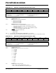
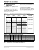
REGISTER 23-2: CONFIG2L: CONFIGURATION REGISTER 2 LOW
U-0 U-0 U-0 R/P-1 R/P-1 R/P-1 R/P-1 R/P-1
— — —BORV1
(1)
BORV0
(1)
BOREN1
(2)
BOREN0
(2)
PWRTEN
(2)
bit 7 bit 0
Legend:
R = Readable bit P = Programmable bit U = Unimplemented bit, read as ‘0’
-n = Value when device is unprogrammed x = Bit is unknown
bit 7-5 Unimplemented: Read as ‘0’
bit 4-3 BORV<1:0>: Brown-out Reset Voltage bits
(1)
11 = VBOR set to 1.8V nominal
10 = V
BOR set to 2.2V nominal
01 = V
BOR set to 2.7V nominal
00 = V
BOR set to 3.0V nominal
bit 2-1 BOREN<1:0>: Brown-out Reset Enable bits
(2)
11 = Brown-out Reset enabled in hardware only (SBOREN is disabled)
10 = Brown-out Reset enabled in hardware only and disabled in Sleep mode
(SBOREN is disabled)
01 = Brown-out Reset enabled and controlled by software (SBOREN is enabled)
00 = Brown-out Reset disabled in hardware and software
bit 0 PWRTEN
: Power-up Timer Enable bit
(2)
1 = PWRT disabled
0 = PWRT enabled
Note 1: See Section 26.1 “DC Characteristics: Supply Voltage” for specifications.
2: The Power-up Timer is decoupled from Brown-out Reset, allowing these features to be independently controlled.
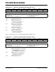
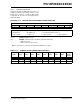
REGISTER 23-3: CONFIG2H: CONFIGURATION REGISTER 2 HIGH
U-0 U-0 U-0 R/P-1 R/P-1 R/P-1 R/P-1 R/P-1
— — — WDTPS3 WDTPS2 WDTPS1 WDTPS0 WDTEN
bit 7 bit 0
Legend:
R = Readable bit P = Programmable bit U = Unimplemented bit, read as ‘0’
-n = Value when device is unprogrammed x = Bit is unknown
bit 7-5 Unimplemented: Read as ‘0’
bit 4-1 WDTPS<3:0>: Watchdog Timer Postscale Select bits
1111 = 1:32,768
1110 = 1:16,384
1101 = 1:8,192
1100 = 1:4,096
1011 = 1:2,048
1010 = 1:1,024
1001 = 1:512
1000 = 1:256
0111 = 1:128
0110 = 1:64
0101 = 1:32
0100 = 1:16
0011 = 1:8
0010 = 1:4
0001 = 1:2
0000 = 1:1
bit 0 WDTEN: Watchdog Timer Enable bit
1 = WDT is always enabled. SWDTEN bit has no effect
0 = WDT is controlled by SWDTEN bit of the WDTCON register