
Datasheet


2010 Microchip Technology Inc. DS41303G-page 291
PIC18F2XK20/4XK20
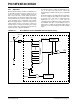
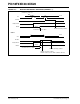
FIGURE 21-2: VOLTAGE REFERENCE OUTPUT BUFFER EXAMPLE
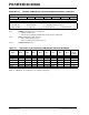
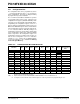
REGISTER 21-1: CVRCON: COMPARATOR VOLTAGE REFERENCE CONTROL REGISTER
R/W-0 R/W-0 R/W-0 R/W-0 R/W-0 R/W-0 R/W-0 R/W-0
CVREN CVROE
(1)
CVRR CVRSS CVR3 CVR2 CVR1 CVR0
bit 7 bit 0
Legend:
R = Readable bit W = Writable bit U = Unimplemented bit, read as ‘0’
-n = Value at POR ‘1’ = Bit is set ‘0’ = Bit is cleared x = Bit is unknown
bit 7 CVREN: Comparator Voltage Reference Enable bit
1 =CV
REF circuit powered on
0 =CV
REF circuit powered down
bit 6 CVROE: Comparator V
REF Output Enable bit
(1)
1 =CVREF voltage level is also output on the CVREF pin
0 =CV
REF voltage is disconnected from the CVREF pin
bit 5 CVRR: Comparator V
REF Range Selection bit
1 = 0 to 0.667 CV
RSRC, with CVRSRC/24 step size (low range)
0 =0.25 CV
RSRC to 0.75 CVRSRC, with CVRSRC/32 step size (high range)
bit 4 CVRSS: Comparator VREF Source Selection bit
1 = Comparator reference source, CVRSRC = (VREF+) – (VREF-)
0 = Comparator reference source, CV
RSRC = VDD – VSS
bit 3-0 CVR<3:0>: Comparator VREF Value Selection bits (0 (CVR<3:0>) 15)
When CVRR =
1:
CV
REF = ((CVR<3:0>)/24) (CVRSRC) + VREF-
When CVRR =
0:
CV
REF = (CVRSRC/4) + ((CVR<3:0>)/32) (CVRSRC) + VREF-
Note 1: CVROE overrides the TRISA<2> bit setting.
Buffered CVREF Output
+
–
CVREF
Module
Voltage
Reference
Output
Impedance
R
(1)
CVREF
Note 1: R is dependent upon the voltage reference Configuration bits, CVR<3:0> and CVRR.
PIC18F2XK20/4XK20