
Datasheet

2010 Microchip Technology Inc. DS41303G-page 263
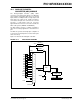
PIC18F2XK20/4XK20
18.4.2.3 EUSART Synchronous Slave
Reception
The operation of the Synchronous Master and Slave
modes is identical (Section 18.4.1.6 “Synchronous
Master Reception”), with the following exceptions:
• Sleep
• CREN bit is always set, therefore the receiver is
never Idle
• SREN bit, which is a “don't care” in Slave mode
A character may be received while in Sleep mode by
setting the CREN bit prior to entering Sleep. Once the
word is received, the RSR register will transfer the data
to the RCREG register. If the RCIE enable bit is set, the
interrupt generated will wake the device from Sleep
and execute the next instruction. If the GIE bit is also
set, the program will branch to the interrupt vector.
18.4.2.4 Synchronous Slave Reception
Set-up:
1. Set the SYNC and SPEN bits and clear the
CSRC bit.
2. Set the RX/DT and TX/CK TRIS controls to ‘1’.
3. If using interrupts, ensure that the GIE and PEIE
bits of the INTCON register are set and set the
RCIE bit.
4. If 9-bit reception is desired, set the RX9 bit.
5. Set the CREN bit to enable reception.
6. The RCIF bit will be set when reception is
complete. An interrupt will be generated if the
RCIE bit was set.
7. If 9-bit mode is enabled, retrieve the Most
Significant bit from the RX9D bit of the RCSTA
register.
8. Retrieve the 8 Least Significant bits from the
receive FIFO by reading the RCREG register.
9. If an overrun error occurs, clear the error by
either clearing the CREN bit of the RCSTA
register or by clearing the SPEN bit which resets
the EUSART.
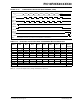
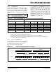
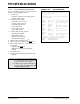
TABLE 18-10: REGISTERS ASSOCIATED WITH SYNCHRONOUS SLAVE RECEPTION
Name Bit 7 Bit 6 Bit 5 Bit 4 Bit 3 Bit 2 Bit 1 Bit 0
Reset
Values
on page
INTCON GIE/GIEH PEIE/GIEL TMR0IE INT0IE RBIE TMR0IF INT0IF RBIF 59
PIR1 PSPIF
(1)
ADIF RCIF TXIF SSPIF CCP1IF TMR2IF TMR1IF 62
PIE1 PSPIE
(1)
ADIE RCIE TXIE SSPIE CCP1IE TMR2IE TMR1IE 62
IPR1
PSPIP
(1)
ADIP RCIP TXIP SSPIP CCP1IP TMR2IP TMR1IP 62
RCSTA SPEN RX9 SREN CREN ADDEN FERR OERR RX9D 61
RCREG EUSART Receive Register 61
TXSTA CSRC
TX9 TXEN SYNC SENDB BRGH TRMT TX9D 61
BAUDCON
ABDOVF RCIDL DTRXP CKTXP BRG16 — WUE ABDEN 61
SPBRGH EUSART Baud Rate Generator Register, High Byte 61
SPBRG EUSART Baud Rate Generator Register, Low Byte 61
Legend: — = unimplemented, read as ‘0’. Shaded cells are not used for synchronous slave reception.
Note 1: Reserved in 28-pin devices; always maintain these bits clear.