
Datasheet


PIC18F2XK20/4XK20
DS41303G-page 170 2010 Microchip Technology Inc.
15.1 Timer3 Operation
Timer3 can operate in one of three modes:
•Timer
• Synchronous Counter
• Asynchronous Counter
The operating mode is determined by the clock select
bit, TMR3CS of the T3CON register. When TMR3CS is
cleared (= 0), Timer3 increments on every internal
instruction cycle (FOSC/4). When the bit is set, Timer3
increments on every rising edge of the Timer1 external
clock input or the Timer1 oscillator, if enabled.
As with Timer1, the digital circuitry associated with the
RC1/T1OSI and RC0/T1OSO/T13CKI pins is disabled
when the Timer1 oscillator is enabled. This means the
values of TRISC<1:0> are ignored and the pins are
read as ‘0’.
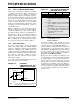
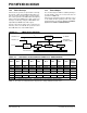
FIGURE 15-1: TIMER3 BLOCK DIAGRAM
T3SYNC
TMR3CS
T3CKPS<1:0>
Sleep Input
T1OSCEN
(1)
FOSC/4
Internal
Clock
Prescaler
1, 2, 4, 8
Synchronize
Detect
1
0
2
T1OSO/T13CKI
T1OSI
1
0
TMR3ON
TMR3L
Set
TMR3IF
on Overflow
TMR3
High Byte
Timer1 Oscillator
Note 1: When enable bit, T1OSCEN, is cleared, the inverter and feedback resistor are turned off to eliminate power drain.
On/Off
Timer3
CCP1/CCP2 Special Event Trigger
CCP1/CCP2 Select from T3CON<6,3>
Clear TMR3
Timer1 Clock Input