
Datasheet

2010 Microchip Technology Inc. DS41303G-page 307
PIC18F2XK20/4XK20
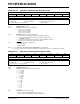
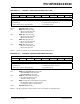
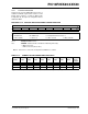
REGISTER 23-12: DEVID1: DEVICE ID REGISTER 1 FOR PIC18F2XK20/4XK20
RRRRRRRR
DEV2 DEV1 DEV0 REV4 REV3 REV2 REV1 REV0
bit 7 bit 0
Legend:
R = Readable bit U = Unimplemented bit, read as ‘0’
-n = Value when device is unprogrammed C = Clearable only bit
bit 7-5 DEV<2:0>: Device ID bits
000 = PIC18F46K20
001 = PIC18F26K20
010 = PIC18F45K20
011 = PIC18F25K20
100 = PIC18F44K20
101 = PIC18F24K20
110 = PIC18F43K20
111 = PIC18F23K20
bit 4-0 REV<4:0>: Revision ID bits
These bits are used to indicate the device revision.
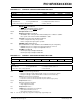
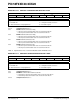
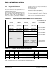
REGISTER 23-13: DEVID2: DEVICE ID REGISTER 2 FOR PIC18F2XK20/4XK20
RRRRRRRR
DEV10 DEV9 DEV8 DEV7 DEV6 DEV5 DEV4 DEV3
bit 7 bit 0
Legend:
R = Readable bit U = Unimplemented bit, read as ‘0’
-n = Value when device is unprogrammed C = Clearable only bit
bit 7-0 DEV<10:3>: Device ID bits
These bits are used with the DEV<2:0> bits in the Device ID Register 1 to identify the
part number.
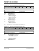
0010 0000 = PIC18F2XK20/4XK20 devices
Note 1: These values for DEV<10:3> may be shared with other devices. The specific device is always identified
by using the entire DEV<10:0> bit sequence.