
Datasheet

2010 Microchip Technology Inc. DS41303G-page 287
PIC18F2XK20/4XK20
20.8 Additional Comparator Features
There are two additional comparator features:
• Simultaneous read of comparator outputs
• Internal reference selection
20.8.1 SIMULTANEOUS COMPARATOR
OUTPUT READ
The MC1OUT and MC2OUT bits of the CM2CON1
register are mirror copies of both comparator outputs.
The ability to read both outputs simultaneously from a
single register eliminates the timing skew of reading
separate registers.
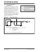
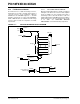
20.8.2 INTERNAL REFERENCE
SELECTION
There are two internal voltage references available to
the non-inverting input of each comparator. One of
these is the 1.2V Fixed Voltage Reference (FVR) and
the other is the variable Comparator Voltage Reference
(CV
REF). The CxRSEL bit of the CM2CON register
determines which of these references is routed to the
Comparator Voltage reference output (CXVREF). Fur-
ther routing to the comparator is accomplished by the
CxR bit of the CMxCON0 register. See Section 21.1
“Comparator Voltage Reference” and Figure 20-2
and Figure 20-3 for more detail.
Note 1: Obtaining the status of C1OUT or C2OUT
by reading CM2CON1 does not affect the
comparator interrupt mismatch registers.
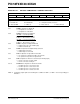
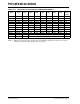
REGISTER 20-3: CM2CON1: COMPARATOR 2 CONTROL REGISTER 1
R-0 R-0 R/W-0 R/W-0 U-0 U-0 U-0 U-0
MC1OUT MC2OUT C1RSEL C2RSEL — — — —
bit 7 bit 0
Legend:
R = Readable bit W = Writable bit U = Unimplemented bit, read as ‘0’
-n = Value at POR ‘1’ = Bit is set ‘0’ = Bit is cleared x = Bit is unknown
bit 7 MC1OUT: Mirror Copy of C1OUT bit
bit 6 MC2OUT: Mirror Copy of C2OUT bit
bit 5 C1RSEL: Comparator C1 Reference Select bit
1 = CV
REF routed to C1VREF input
0 = FVR (1.2 Volt fixed voltage reference) routed to C1VREF input
bit 4 C2RSEL: Comparator C2 Reference Select bit
1 = CVREF routed to C2VREF input
0 = FVR (1.2 Volt fixed voltage reference) routed to C2V
REF input
bit 3-0 Unimplemented: Read as ‘0’