
Datasheet


PIC18F2XK20/4XK20
DS41303G-page 268 2010 Microchip Technology Inc.
19.2 ADC Operation
19.2.1 STARTING A CONVERSION
To enable the ADC module, the ADON bit of the
ADCON0 register must be set to a ‘1’. Setting the GO/
DONE bit of the ADCON0 register to a ‘1’ will, depend-
ing on the ACQT bits of the ADCON2 register, either
immediately start the Analog-to-Digital conversion or
start an acquisition delay followed by the Analog-to-
Digital conversion.
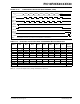
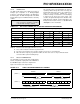
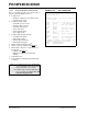
Figure 19-3 shows the operation of the A/D converter
after the GO bit has been set and the ACQT<2:0> bits
are cleared. A conversion is started after the following
instruction to allow entry into SLEEP mode before the
conversion begins.
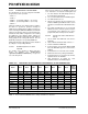
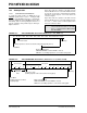
Figure 19-4 shows the operation of the A/D converter
after the GO bit has been set and the ACQT<2:0> bits
are set to ‘010’ which selects a 4 T
AD acquisition time
before the conversion starts.
FIGURE 19-3: A/D CONVERSION TAD CYCLES (ACQT<2:0> = 000, TACQ = 0)
FIGURE 19-4: A/D CONVERSION T
AD CYCLES (ACQT<2:0> = 010, TACQ = 4 TAD)
Note: The GO/DONE bit should not be set in the
same instruction that turns on the ADC.
Refer to Section 19.2.9 “A/D Conver-
sion Procedure”.
TAD1 TAD2
TAD3
TAD4 TAD5
TAD6 TAD7
TAD8
TAD11
Set GO bit
Holding capacitor is disconnected from analog input (typically 100 ns)
TAD9 TAD10
TCY - TAD
ADRESH:ADRESL is loaded, GO bit is cleared,
ADIF bit is set, holding capacitor is connected to analog input.
Conversion starts
b0
b9
b6
b5
b4
b3
b2
b1
b8
b7
On the following cycle:
2 TAD
Discharge
1
2
3 4
5
6 7
8 11
Set GO bit
(Holding capacitor is disconnected from analog input)
9 10
Conversion starts
1
2
3
4
(Holding capacitor continues
acquiring input)
T
ACQT Cycles
TAD Cycles
Automatic
Acquisition
Time
b0b9
b6
b5 b4
b3
b2
b1
b8
b7
ADRESH:ADRESL is loaded, GO bit is cleared,
ADIF bit is set, holding capacitor is connected to analog input.
On the following cycle:
2 TAD
Discharge