
Datasheet

2010 Microchip Technology Inc. DS41303G-page 127
PIC18F2XK20/4XK20
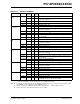
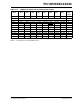
10.4 PORTC, TRISC and LATC
Registers
PORTC is an 8-bit wide, bidirectional port. The corre-
sponding data direction register is TRISC. Setting a
TRISC bit (= 1) will make the corresponding PORTC
pin an input (i.e., disable the output driver). Clearing a
TRISC bit (= 0) will make the corresponding PORTC
pin an output (i.e., enable the output driver and put the
contents of the output latch on the selected pin).
The Data Latch register (LATC) is also memory
mapped. Read-modify-write operations on the LATC
register read and write the latched output value for
PORTC.
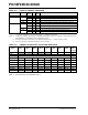
PORTC is multiplexed with several peripheral functions
(Table 10-5). The pins have Schmitt Trigger input buf-
fers. RC1 is the default configuration for the CCP2
peripheral pin. The CCP2 function can be relocated to
the RB3 pin by clearing the CCP2MX bit of Configura-
tion Word CONFIG3H. The default state of the
CCP2MX Configuration bit is ‘1’.
When enabling peripheral functions, care should be
taken in defining TRIS bits for each PORTC pin. The
EUSART and MSSP peripherals override the TRIS bit
to make a pin an output or an input, depending on the
peripheral configuration. Refer to the corresponding
peripheral section for additional information.
The contents of the TRISC register are affected by
peripheral overrides. Reading TRISC always returns
the current contents, even though a peripheral device
may be overriding one or more of the pins.
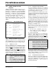
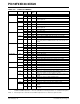
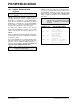
EXAMPLE 10-3: INITIALIZING PORTC
Note: On a Power-on Reset, these pins are con-
figured as digital inputs.
CLRF PORTC ; Initialize PORTC by
; clearing output
; data latches
CLRF LATC ; Alternate method
; to clear output
; data latches
MOVLW 0CFh ; Value used to
; initialize data
; direction
MOVWF TRISC ; Set RC<3:0> as inputs
; RC<5:4> as outputs
; RC<7:6> as inputs