
Datasheet


PIC18F2XK20/4XK20
DS41303G-page 114 2010 Microchip Technology Inc.
9.6 PIE Registers
The PIE registers contain the individual enable bits for
the peripheral interrupts. Due to the number of periph-
eral interrupt sources, there are two Peripheral Interrupt
Enable registers (PIE1 and PIE2). When IPEN = 0, the
PEIE bit must be set to enable any of these peripheral
interrupts.
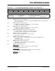
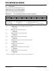
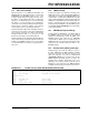
REGISTER 9-6: PIE1: PERIPHERAL INTERRUPT ENABLE (FLAG) REGISTER 1
R/W-0 R/W-0 R/W-0 R/W-0 R/W-0 R/W-0 R/W-0 R/W-0
PSPIE
(1)
ADIE RCIE TXIE SSPIE CCP1IE TMR2IE TMR1IE
bit 7 bit 0
Legend:
R = Readable bit W = Writable bit U = Unimplemented bit, read as ‘0’
-n = Value at POR ‘1’ = Bit is set ‘0’ = Bit is cleared x = Bit is unknown
bit 7 PSPIE: Parallel Slave Port Read/Write Interrupt Enable bit
(1)
1 = Enables the PSP read/write interrupt
0 = Disables the PSP read/write interrupt
bit 6 ADIE: A/D Converter Interrupt Enable bit
1 = Enables the A/D interrupt
0 = Disables the A/D interrupt
bit 5 RCIE: EUSART Receive Interrupt Enable bit
1 = Enables the EUSART receive interrupt
0 = Disables the EUSART receive interrupt
bit 4 TXIE: EUSART Transmit Interrupt Enable bit
1 = Enables the EUSART transmit interrupt
0 = Disables the EUSART transmit interrupt
bit 3 SSPIE: Master Synchronous Serial Port Interrupt Enable bit
1 = Enables the MSSP interrupt
0 = Disables the MSSP interrupt
bit 2 CCP1IE: CCP1 Interrupt Enable bit
1 = Enables the CCP1 interrupt
0 = Disables the CCP1 interrupt
bit 1 TMR2IE: TMR2 to PR2 Match Interrupt Enable bit
1 = Enables the TMR2 to PR2 match interrupt
0 = Disables the TMR2 to PR2 match interrupt
bit 0 TMR1IE: TMR1 Overflow Interrupt Enable bit
1 = Enables the TMR1 overflow interrupt
0 = Disables the TMR1 overflow interrupt
Note 1: The PSPIE bit is unimplemented on 28-pin devices and will read as ‘0’.