
Datasheet


PIC18F45J10 FAMILY
DS39682E-page 238 © 2009 Microchip Technology Inc.
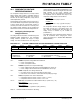
REGISTER 21-3: CONFIG2L: CONFIGURATION REGISTER 2 LOW (BYTE ADDRESS 300002h)
R/WO-1 R/WO-1 U-0 U-0 U-0 R/WO-1 R/WO-1 R/WO-1
IESO FCMEN
— — — FOSC2 FOSC1 FOSC0
bit 7 bit 0
Legend:
R = Readable bit WO = Write Once bit U = Unimplemented bit, read as ‘0’
-n = Value when device is unprogrammed ‘1’ = Bit is set ‘0’ = Bit is cleared
bit 7 IESO: Two-Speed Start-up (Internal/External Oscillator Switchover) Control bit
1 = Two-Speed Start-up enabled
0 = Two-Speed Start-up disabled
bit 6 FCMEN: Fail-Safe Clock Monitor Enable bit
1 = Fail-Safe Clock Monitor enabled
0 = Fail-Safe Clock Monitor disabled
bit 5-3 Unimplemented: Read as ‘0’
bit 2 FOSC2: Default/Reset System Clock Select bit
1 = Clock selected by FOSC<1:0> as system clock is enabled when OSCCON<1:0> = 00
0 = INTRC enabled as system clock when OSCCON<1:0> = 00
bit 1-0 FOSC<1:0>: Oscillator Selection bits
11 = EC oscillator, PLL enabled and under software control, CLKO function on OSC2
10 = EC oscillator, CLKO function on OSC2
01 = HS oscillator, PLL enabled and under software control
00 = HS oscillator