
Datasheet


© 2009 Microchip Technology Inc. DS39682E-page 213
PIC18F45J10 FAMILY
17.4.2 EUSART SYNCHRONOUS SLAVE
RECEPTION
The operation of the Synchronous Master and Slave
modes is identical, except in the case of Sleep, or any
Idle mode and bit, SREN, which is a “don’t care” in
Slave mode.
If receive is enabled by setting the CREN bit prior to
entering Sleep or any Idle mode, then a word may be
received while in this low-power mode. Once the word
is received, the RSR register will transfer the data to the
RCREG register; if the RCIE enable bit is set, the inter-
rupt generated will wake the chip from the low-power
mode. If the global interrupt is enabled, the program will
branch to the interrupt vector.
To set up a Synchronous Slave Reception:
1. Enable the synchronous master serial port by
setting bits, SYNC and SPEN, and clearing bit,
CSRC.
2. If interrupts are desired, set enable bit, RCIE.
3. If 9-bit reception is desired, set bit, RX9.
4. To enable reception, set enable bit, CREN.
5. Flag bit, RCIF, will be set when reception is
complete. An interrupt will be generated if
enable bit, RCIE, was set.
6. Read the RCSTA register to get the 9th bit (if
enabled) and determine if any error occurred
during reception.
7. Read the 8-bit received data by reading the
RCREG register.
8. If any error occurred, clear the error by clearing
bit, CREN.
9. If using interrupts, ensure that the GIE and PEIE
bits in the INTCON register (INTCON<7:6>) are
set.
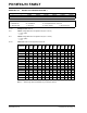
TABLE 17-10: REGISTERS ASSOCIATED WITH SYNCHRONOUS SLAVE RECEPTION
Name Bit 7 Bit 6 Bit 5 Bit 4 Bit 3 Bit 2 Bit 1 Bit 0
Reset
Values
on page
INTCON GIE/GIEH PEIE/GIEL TMR0IE INT0IE RBIE TMR0IF INT0IF RBIF 47
PIR1
PSPIF
(1)
ADIF RCIF TXIF SSP1IF CCP1IF TMR2IF TMR1IF 49
PIE1 PSPIE
(1)
ADIE RCIE TXIE SSP1IE CCP1IE TMR2IE TMR1IE 49
IPR1 PSPIP
(1)
ADIP RCIP TXIP SSP1IP CCP1IP TMR2IP TMR1IP 49
RCSTA SPEN RX9 SREN CREN
ADDEN FERR OERR RX9D 49
RCREG EUSART Receive Register 49
TXSTA CSRC TX9 TXEN SYNC SENDB BRGH TRMT TX9D 49
BAUDCON
ABDOVF RCIDL —SCKPBRG16— WUE ABDEN 49
SPBRGH EUSART Baud Rate Generator Register High Byte 49
SPBRG EUSART Baud Rate Generator Register Low Byte 49
Legend: — = unimplemented, read as ‘0’. Shaded cells are not used for synchronous slave reception.
Note 1: These bits are not implemented on 28-pin devices and should be read as ‘0’.