
Datasheet


© 2009 Microchip Technology Inc. DS39682E-page 163
PIC18F45J10 FAMILY
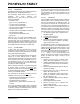
REGISTER 16-6: SSPxCON2: MSSPx CONTROL REGISTER 2 (I
2
C™ SLAVE MODE)
R/W-0 R/W-0 R/W-0 R/W-0 R/W-0 R/W-0 R/W-0 R/W-0
GCEN ACKSTAT ADMSK5 ADMSK4 ADMSK3 ADMSK2 ADMSK1 SEN
(1)
bit 7 bit 0
Legend:
R = Readable bit W = Writable bit U = Unimplemented bit, read as ‘0’
-n = Value at POR ‘1’ = Bit is set ‘0’ = Bit is cleared x = Bit is unknown
bit 7 GCEN: General Call Enable bit
1 = Enable interrupt when a general call address (0000h) is received in the SSPxSR
0 = General call address disabled
bit 6 ACKSTAT: Acknowledge Status bit
Unused in Slave mode.
bit 5-2 ADMSK<5:2>: Slave Address Mask Select bits
1 = Masking of corresponding bits of SSPxADD enabled
0 = Masking of corresponding bits of SSPxADD disabled
bit 1 ADMSK1: Slave Address Least Significant bit(s) Mask Select bit
In 7-
Bit Addressing mode:
1 = Masking of SSPxADD<1> only enabled
0 = Masking of SSPxADD<1> only disabled
In 10-
Bit Addressing mode:
1 = Masking of SSPxADD<1:0> enabled
0 = Masking of SSPxADD<1:0> disabled
bit 0 SEN: Stretch Enable bit
(1)
1 = Clock stretching is enabled for both slave transmit and slave receive (stretch enabled)
0 = Clock stretching is disabled
Note 1: If the I
2
C module is active, this bit may not be set (no spooling) and the SSPxBUF may not be written (or
writes to the SSPxBUF are disabled).