
Datasheet


© 2009 Microchip Technology Inc. DS39682E-page 107
PIC18F45J10 FAMILY
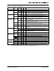
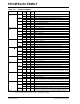
10.5 PORTD, TRISD and LATD
Registers
PORTD is an 8-bit wide, bidirectional port. The corre-
sponding Data Direction register is TRISD. Setting a
TRISD bit (= 1) will make the corresponding PORTD
pin an input (i.e., put the corresponding output driver in
a high-impedance mode). Clearing a TRISD bit (= 0)
will make the corresponding PORTD pin an output (i.e.,
put the contents of the output latch on the selected pin).
The Data Latch register (LATD) is also memory
mapped. Read-modify-write operations on the LATD
register read and write the latched output value for
PORTD.
All pins on PORTD are implemented with Schmitt Trigger
input buffers. Each pin is individually configurable as an
input or output.
Three of the PORTD pins are multiplexed with outputs
P1B, P1C and P1D of the Enhanced CCP module. The
operation of these additional PWM output pins is
covered in greater detail in Section 15.0 “Enhanced
Capture/Compare/PWM (ECCP) Module”.
PORTD can also be configured as an 8-bit wide micro-
processor port (Parallel Slave Port) by setting control
bit, PSPMODE (TRISE<4>). In this mode, the input
buffers are TTL. See Section 10.7 “Parallel Slave
Port” for additional information on the Parallel Slave
Port (PSP).
EXAMPLE 10-5: INITIALIZING PORTD
Note: PORTD is only available in 40/44-pin
devices.
Note: On a Power-on Reset, these pins are
configured as digital inputs.
Note: When the Enhanced PWM mode is used
with either dual or quad outputs, the PSP
functions of PORTD are automatically
disabled.
CLRF PORTD ; Initialize PORTD by
; clearing output
; data latches
CLRF LATD ; Alternate method
; to clear output
; data latches
MOVLW 0CFh ; Value used to
; initialize data
; direction
MOVWF TRISD ; Set RD<3:0> as inputs
; RD<5:4> as outputs
; RD<7:6> as inputs