
Datasheet


© 2009 Microchip Technology Inc. DS39682E-page 103
PIC18F45J10 FAMILY
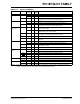
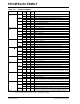
TABLE 10-6: SUMMARY OF REGISTERS ASSOCIATED WITH PORTB
Name Bit 7 Bit 6 Bit 5 Bit 4 Bit 3 Bit 2 Bit 1 Bit 0
Reset
Values
on page
PORTB RB7 RB6 RB5 RB4 RB3 RB2 RB1 RB0 50
LATB PORTB Data Latch Register (Read and Write to Data Latch) 50
TRISB PORTB Data Direction Control Register 50
INTCON
GIE/GIEH PEIE/GIEL TMR0IE INT0IE RBIE TMR0IF INT0IF RBIF 47
INTCON2 RBPU
INTEDG0 INTEDG1 INTEDG2 — TMR0IP —RBIP47
INTCON3 INT2IP INT1IP
—INT2IEINT1IE— INT2IF INT1IF 47
ADCON1 — — VCFG1 VCFG0 PCFG3 PCFG2 PCFG1 PCFG0 48
Legend: — = unimplemented, read as ‘0’. Shaded cells are not used by PORTB.