
Datasheet


© 2009 Microchip Technology Inc. DS39682E-page 101
PIC18F45J10 FAMILY
10.3 PORTB, TRISB and LATB
Registers
PORTB is an 8-bit wide, bidirectional port. The corre-
sponding Data Direction register is TRISB. Setting a
TRISB bit (= 1) will make the corresponding PORTB
pin an input (i.e., put the corresponding output driver in
a high-impedance mode). Clearing a TRISB bit (= 0)
will make the corresponding PORTB pin an output (i.e.,
put the contents of the output latch on the selected pin).
The Data Latch register (LATB) is also memory
mapped. Read-modify-write operations on the LATB
register read and write the latched output value for
PORTB.
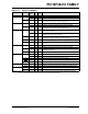
EXAMPLE 10-3: INITIALIZING PORTB
Each of the PORTB pins has a weak internal pull-up. A
single control bit can turn on all the pull-ups. This is
performed by clearing bit, RBPU (INTCON2<7>). The
weak pull-up is automatically turned off when the port
pin is configured as an output. The pull-ups are
disabled on a Power-on Reset.
Four of the PORTB pins (RB<7:4>) have an interrupt-
on-change feature. Only pins configured as inputs can
cause this interrupt to occur (i.e., any RB<7:4> pin
configured as an output is excluded from the interrupt-
on-change comparison). The input pins (of RB<7:4>)
are compared with the old value latched on the last
read of PORTB. The “mismatch” outputs of RB<7:4>
are ORed together to generate the RB Port Change
Interrupt with Flag bit, RBIF (INTCON<0>).
This interrupt can wake the device from Sleep mode or
any of the Idle modes. The user, in the Interrupt Service
Routine, can clear the interrupt in the following manner:
a) Any read or write of PORTB (except with the
MOVFF (ANY), PORTB instruction).
b) Clear flag bit, RBIF.
A mismatch condition will continue to set flag bit, RBIF.
Reading PORTB will end the mismatch condition and
allow flag bit, RBIF, to be cleared.
The interrupt-on-change feature is recommended for
wake-up on key depression operation and operations
where PORTB is only used for the interrupt-on-change
feature. Polling of PORTB is not recommended while
using the interrupt-on-change feature.
RB3 can be configured by the Configuration bit,
CCP2MX, as the alternate peripheral pin for the CCP2
module (CCP2MX = 0).
The RB5 pin is multiplexed with the Timer0 module
clock input and one of the comparator outputs to
become the RB5/KBI1/T0CKI/C1OUT pin.
Note: On a Power-on Reset, RB<4:0> are
configured as analog inputs by default and
read as ‘0’; RB<7:5> are configured as
digital inputs.
CLRF PORTB ; Initialize PORTB by
; clearing output
; data latches
CLRF LATB ; Alternate method
; to clear output
; data latches
MOVLW 0Fh ; Set RB<4:0> as
MOVWF ADCON1 ; digital I/O pins
MOVLW 0CFh ; Value used to
; initialize data
; direction
MOVWF TRISB ; Set RB<3:0> as inputs
; RB<5:4> as outputs
; RB<7:6> as inputs