
Datasheet


© 2009 Microchip Technology Inc. DS39682E-page 99
PIC18F45J10 FAMILY
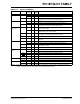
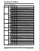
TABLE 10-3: PORTA I/O SUMMARY
Pin Function
TRIS
Setting
I/O
I/O
Type
Description
RA0/AN0 RA0 0 O DIG LATA<0> data output; not affected by analog input.
1 I TTL PORTA<0> data input; disabled when analog input enabled.
AN0 1 I ANA A/D Input Channel 0 and Comparator C1- input. Default input
configuration on POR; does not affect digital output.
RA1/AN1 RA1 0 O DIG LATA<1> data output; not affected by analog input.
1 I TTL PORTA<1> data input; disabled when analog input enabled.
AN1 1 I ANA A/D Input Channel 1 and Comparator C2- input. Default input
configuration on POR; does not affect digital output.
RA2/AN2/
V
REF-/CVREF
RA2 0 O DIG LATA<2> data output; not affected by analog input. Disabled when
CV
REF output enabled.
1 I TTL PORTA<2> data input. Disabled when analog functions enabled;
disabled when CV
REF output enabled.
AN2 1 I ANA A/D Input Channel 2 and Comparator C2+ input. Default input
configuration on POR; not affected by analog output.
V
REF- 1 I ANA A/D and comparator voltage reference low input.
CV
REF x O ANA Comparator voltage reference output. Enabling this feature disables
digital I/O.
RA3/AN3/V
REF+RA30 O DIG LATA<3> data output; not affected by analog input.
1 I TTL PORTA<3> data input; disabled when analog input enabled.
AN3 1 I ANA A/D Input Channel 3 and Comparator C1+ input. Default input
configuration on POR.
V
REF+ 1 I ANA A/D and comparator voltage reference high input.
RA5/AN4/SS
1/
C2OUT
RA5 0 O DIG LATA<5> data output; not affected by analog input.
1 I TTL PORTA<5> data input; disabled when analog input enabled.
AN4 1 I ANA A/D Input Channel 4. Default configuration on POR.
SS
1 1 I TTL Slave select input for MSSP1 (MSSP1 module).
C2OUT 0 O DIG Comparator 2 output; takes priority over port data.
OSC2/CLKO OSC2 x O ANA Main oscillator feedback output connection (HS mode).
CLKO x O DIG System cycle clock output (F
OSC/4) in RC and EC Oscillator modes.
OSC1/CLKI OSC1 x I ANA Main oscillator input connection.
CLKI x I ANA Main clock input connection.
Legend: DIG = Digital level output; TTL = TTL input buffer; ST = Schmitt Trigger input buffer; ANA = Analog level input/output;
x = Don’t care (TRIS bit does not affect port direction or is overridden for this option).