
Datasheet


© 2007 Microchip Technology Inc. Preliminary DS39625C-page 133
PIC18F2585/2680/4585/4680
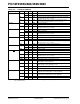
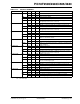
TABLE 10-3: PORTB I/O SUMMARY
Pin Name Function I/O TRIS Buffer Description
RB0/INT0/FLT0/AN10 RB0 OUT 0 DIG LATB<0> data output.
IN 1 TTL PORTB<0> data input. Weak pull-up available only in this mode.
INT0 IN 1 ST External interrupt 0 input.
FLT0 IN 1 ST Enhanced PWM Fault input.
AN10 IN 1 ANA A/D input channel 10. Enabled on POR, this analog input overrides
the digital input (read as clear – low level).
RB1/INT1/AN8 RB1 OUT 0 DIG LATB<1> data output.
IN 1 TTL PORTB<1> data input. Weak pull-up available only in this mode.
INT1 IN 1 ST External interrupt 1 input.
AN8 IN 1 ANA A/D input channel 8. Enabled on POR, this analog input overrides
the digital input (read as clear – low level).
RB2/INT2/CANTX RB2 OUT x DIG LATB<2> data output.
IN 1 TTL PORTB<2> data input. Weak pull-up available only in this mode.
INT2 IN 1 ST External interrupt 2 input.
CANTX OUT 1 DIG CAN transmit signal output. The CAN interface overrides the
TRIS<2> control when enabled.
RB3/CANRX RB3 OUT 0 DIG LATB<3> data output.
IN 1 TTL PORTB<3> data input. Weak pull-up available only in this mode.
CANRX IN 1 ST CAN receive signal input. Pin must be configured as a digital input by
setting TRISB<3>.
RB4/KBI0/AN9 RB4 OUT 0 DIG LATB<4> data output.
IN 1 TTL PORTB<4> data input. Weak pull-up available only in this mode.
KBI0 IN 1 TTL Interrupt-on-pin change.
AN9 IN 1 ANA A/D input channel 9. Enabled on POR, this analog input overrides
the digital input (read as clear – low level).
RB5/KBI1/PGM RB5 OUT 0 DIG LATB<5> data output.
IN 1 TTL PORTB<5> data input. Weak pull-up available only in this mode.
KBI1 IN 1 TTL Interrupt-on-pin change.
PGM IN x ST Low-Voltage Programming mode entry (ICSP™). Enabling this
function overrides digital output.
RB6/KBI2/PGC RB6 OUT 0 DIG LATB<6> data output.
IN 1 TTL PORTB<6> data input. Weak pull-up available only in this mode.
KBI2 IN 1 TTL Interrupt-on-pin change.
PGC IN x ST Low-Voltage Programming mode entry (ICSP) clock input.
RB7/KBI3/PGD RB7 OUT 0 DIG LATB<7> data output.
IN 1 TTL PORTB<7> data input. Weak pull-up available only in this mode.
KBI3 IN 1 TTL Interrupt-on-pin change.
PGD OUT x DIG Low-Voltage Programming mode entry (ICSP) clock output.
IN x ST Low-Voltage Programming mode entry (ICSP) clock input.
Legend: PWR = Power Supply; OUT = Output; IN = Input; ANA = Analog Signal; DIG = Digital Output; ST = Schmitt Buffer Input;
TTL – TTL Buffer Input