
Datasheet


Table Of Contents
- Power-Managed Modes:
- Flexible Oscillator Structure:
- Special Microcontroller Features:
- Peripheral Highlights:
- ECAN Technology Module Features:
- Pin Diagrams
- Pin Diagrams (Continued)
- Table of Contents
- Most Current Data Sheet
- Errata
- Customer Notification System
- 1.0 Device Overview
- 2.0 Guidelines for Getting Started with PIC18F Microcontrollers
- 3.0 Oscillator Configurations
- 4.0 Power-Managed Modes
- 5.0 Reset
- 5.1 RCON Register
- 5.2 Master Clear Reset (MCLR)
- 5.3 Power-on Reset (POR)
- 5.4 Brown-out Reset (BOR)
- 5.5 Device Reset Timers
- 5.5.1 Power-up Timer (PWRT)
- 5.5.2 Oscillator Start-up Timer (OST)
- 5.5.3 PLL Lock Time-out
- 5.5.4 Time-out Sequence
- TABLE 5-2: Time-out in Various Situations
- FIGURE 5-3: Time-out Sequence on Power-up (MCLR Tied to Vdd, Vdd Rise < Tpwrt)
- FIGURE 5-4: Time-out Sequence on Power-up (MCLR Not Tied to Vdd): Case 1
- FIGURE 5-5: Time-out Sequence on Power-up (MCLR Not Tied to Vdd): Case 2
- FIGURE 5-6: Slow Rise Time (MCLR Tied to Vdd, Vdd Rise > Tpwrt)
- FIGURE 5-7: Time-out Sequence on POR w/PLL Enabled (MCLR Tied to Vdd)
- 5.6 Reset State of Registers
- 6.0 Memory Organization
- 6.1 Program Memory Organization
- 6.2 PIC18 Instruction Cycle
- 6.3 Data Memory Organization
- 6.4 Data Addressing Modes
- 6.5 Program Memory and the Extended Instruction Set
- 6.6 Data Memory and the Extended Instruction Set
- 7.0 Flash Program Memory
- 7.1 Table Reads and Table Writes
- 7.2 Control Registers
- 7.3 Reading the Flash Program Memory
- 7.4 Erasing Flash Program Memory
- 7.5 Writing to Flash Program Memory
- 7.6 Flash Program Operation During Code Protection
- 8.0 Data EEPROM Memory
- 9.0 8 x 8 Hardware Multiplier
- 9.1 Introduction
- 9.2 Operation
- EXAMPLE 9-1: 8 x 8 Unsigned Multiply Routine
- EXAMPLE 9-2: 8 x 8 Signed Multiply Routine
- TABLE 9-1: Performance Comparison for Various Multiply Operations
- EQUATION 9-1: 16 x 16 Unsigned Multiplication Algorithm
- EXAMPLE 9-3: 16 x 16 Unsigned Multiply Routine
- EQUATION 9-2: 16 x 16 Signed Multiplication Algorithm
- EXAMPLE 9-4: 16 x 16 Signed Multiply Routine
- 10.0 Interrupts
- 11.0 I/O Ports
- 12.0 Timer0 Module
- 13.0 Timer1 Module
- 14.0 Timer2 Module
- 15.0 Timer3 Module
- 16.0 Capture/Compare/PWM (CCP) Modules
- Register 16-1: CCP1CON: Capture/Compare/PWM Control Register
- 16.1 CCP Module Configuration
- 16.2 Capture Mode
- 16.3 Compare Mode
- 16.4 PWM Mode
- 17.0 Enhanced Capture/Compare/PWM (ECCP) Module
- Register 17-1: ECCP1CON Register (ECCP1 module, PIC18F4480/4580 Devices)
- 17.1 ECCP Outputs and Configuration
- 17.2 Capture and Compare Modes
- 17.3 Standard PWM Mode
- 17.4 Enhanced PWM Mode
- 18.0 Master Synchronous Serial Port (MSSP) Module
- 18.1 Master SSP (MSSP) Module Overview
- 18.2 Control Registers
- 18.3 SPI Mode
- 18.4 I2C Mode
- FIGURE 18-7: MSSP Block Diagram (I2C™ Mode)
- 18.4.1 Registers
- 18.4.2 Operation
- 18.4.3 Slave Mode
- 18.4.4 Clock Stretching
- 18.4.5 General Call Address Support
- 18.4.6 Master Mode
- 18.4.7 Baud Rate
- 18.4.8 I2C Master Mode Start Condition Timing
- 18.4.9 I2C Master Mode Repeated Start Condition Timing
- 18.4.10 I2C Master Mode Transmission
- 18.4.11 I2C Master Mode Reception
- 18.4.12 Acknowledge Sequence Timing
- 18.4.13 Stop Condition Timing
- 18.4.14 Sleep Operation
- 18.4.15 Effect of a Reset
- 18.4.16 Multi-Master Mode
- 18.4.17 Multi-Master Communication, Bus Collision and Bus Arbitration
- FIGURE 18-25: Bus Collision Timing for Transmit and Acknowledge
- FIGURE 18-26: Bus Collision During Start Condition (SDA Only)
- FIGURE 18-27: Bus Collision During Start Condition (SCL = 0)
- FIGURE 18-28: BRG Reset Due to SDA Arbitration During Start Condition
- FIGURE 18-29: Bus Collision During a Repeated Start Condition (Case 1)
- FIGURE 18-30: Bus Collision During Repeated Start Condition (Case 2)
- FIGURE 18-31: Bus Collision During a Stop Condition (Case 1)
- FIGURE 18-32: Bus Collision During a Stop Condition (Case 2)
- 19.0 Enhanced Universal Synchronous Receiver Transmitter (EUSART)
- Register 19-1: TXSTA: Transmit Status And Control Register
- Register 19-2: RCSTA: Receive Status And Control Register
- Register 19-3: BAUDCON: Baud Rate Control Register
- 19.1 Baud Rate Generator (BRG)
- 19.2 EUSART Asynchronous Mode
- 19.3 EUSART Synchronous Master Mode
- 19.4 EUSART Synchronous Slave Mode
- 20.0 10-Bit Analog-to-Digital Converter (A/D) Module
- Register 20-1: ADCON0: A/D Control Register 0
- Register 20-2: ADCON1: A/D Control Register 1
- Register 20-3: ADCON2: A/D Control Register 2
- FIGURE 20-1: A/D Block Diagram
- FIGURE 20-2: Analog Input Model
- 20.1 A/D Acquisition Requirements
- 20.2 Selecting and Configuring Automatic Acquisition Time
- 20.3 Selecting the A/D Conversion Clock
- 20.4 Operation in Power-Managed Modes
- 20.5 Configuring Analog Port Pins
- 20.6 A/D Conversions
- 20.7 Use of the CCP1 Trigger
- 21.0 Comparator Module
- Register 21-1: CMCON: Comparator Control Register
- 21.1 Comparator Configuration
- 21.2 Comparator Operation
- 21.3 Comparator Reference
- 21.4 Comparator Response Time
- 21.5 Comparator Outputs
- 21.6 Comparator Interrupts
- 21.7 Comparator Operation During Sleep
- 21.8 Effects of a Reset
- 21.9 Analog Input Connection Considerations
- 22.0 Comparator Voltage Reference Module
- 23.0 High/Low-Voltage Detect (HLVD)
- 24.0 ECAN Module
- 24.1 Module Overview
- 24.2 CAN Module Registers
- 24.2.1 CAN Control and Status Registers
- Register 24-1: CANCON: CAN Control Register
- Register 24-2: CANSTAT: CAN Status Register
- EXAMPLE 24-1: Changing to Configuration Mode
- EXAMPLE 24-2: WIN and ICODE Bits Usage in Interrupt Service Routine to Access TX/RX Buffers
- EXAMPLE 24-2: WIN and ICODE Bits Usage in Interrupt Service Routine to Access TX/RX Buffers (Continued)
- Register 24-3: ECANCON: Enhanced CAN Control Register
- Register 24-4: COMSTAT: Communication Status Register
- 24.2.2 Dedicated CAN Transmit Buffer Registers
- Register 24-5: TXBnCON: Transmit Buffer n Control Registers [0 £ n £ 2]
- Register 24-6: TXBnSIDH: Transmit Buffer n Standard Identifier Registers, High Byte [0 £ n £ 2]
- Register 24-7: TXBnSIDL: Transmit Buffer n Standard Identifier Registers, Low Byte [0 £ n £ 2]
- Register 24-8: TXBnEIDH: Transmit Buffer n Extended Identifier Registers, High Byte [0 £ n £ 2]
- Register 24-9: TXBnEIDL: Transmit Buffer n Extended Identifier Registers, Low Byte [0 £ n £ 2]
- Register 24-10: TXBnDm: Transmit Buffer n Data Field Byte m Registers [0 £ n £ 2, 0 £ m £ 7]
- Register 24-11: TXBnDLC: Transmit Buffer n Data Length Code Registers [0 £ n £ 2]
- Register 24-12: TXERRCNT: Transmit Error Count Register
- EXAMPLE 24-3: Transmitting a CAN Message Using Banked Method
- EXAMPLE 24-4: Transmitting a CAN Message Using WIN Bits
- 24.2.3 Dedicated CAN Receive Buffer Registers
- Register 24-13: RXB0CON: Receive Buffer 0 Control Register
- Register 24-14: RXB1CON: Receive Buffer 1 Control Register
- Register 24-15: RXBnSIDH: Receive Buffer n Standard Identifier Registers, High Byte [0 £ n £ 1]
- Register 24-16: RXBnSIDL: Receive Buffer n Standard Identifier Registers, Low Byte [0 £ n £ 1]
- Register 24-17: RXBnEIDH: Receive Buffer n Extended Identifier Registers, High Byte [0 £ n £ 1]
- Register 24-18: RXBnEIDL: Receive Buffer n Extended Identifier Registers, Low Byte [0 £ n £ 1]
- Register 24-19: RXBnDLC: Receive Buffer n Data Length Code Registers [0 £ n £ 1]
- Register 24-20: RXBnDm: Receive Buffer n Data Field Byte m Registers [0 £ n £ 1, 0 £ m £ 7]
- Register 24-21: RXERRCNT: Receive Error Count Register
- EXAMPLE 24-5: Reading a CAN Message
- Register 24-22: BnCON: TX/RX Buffer n Control Registers in Receive Mode [0 £ n £ 5, TXnEN (bsel0
) = 0](1) - Register 24-23: BnCON: TX/RX Buffer n Control Registers in Transmit Mode [0 £ n £ 5, TXnEN (bsel0
) = 1](1) - Register 24-24: BnSIDH: TX/RX Buffer n Standard Identifier Registers, High Byte in Receive Mode [0 £ n £ 5, TXnEN (BSEL0
) = 0](1) - Register 24-25: BnSIDH: TX/RX Buffer n Standard Identifier Registers, High Byte in Transmit Mode [0 £ n £ 5, TXnEN (BSEL0
) = 1](1) - Register 24-26: BnSIDL: TX/RX Buffer n Standard Identifier Registers, Low Byte in Receive Mode [0 £ n £ 5, TXnEN (bsel0
) = 0](1) - Register 24-27: BnSIDL: TX/RX Buffer n Standard Identifier Registers, Low Byte in Receive Mode [0 £ n £ 5, TXnEN (bsel0
) = 1](1) - Register 24-28: BnEIDH: TX/RX Buffer n Extended Identifier Registers, High Byte in Receive Mode [0 £ n £ 5, TXnEN (BSEL0
) = 0](1) - Register 24-29: BnEIDH: TX/RX Buffer n Extended Identifier Registers, High Byte in Transmit Mode [0 £ n £ 5, TXnEN (BSEL0
) = 1](1) - Register 24-30: BnEIDL: TX/RX Buffer n Extended Identifier Registers, Low Byte in Receive Mode [0 £ n £ 5, TXnEN (BSEL
) = 0](1) - Register 24-31: BnEIDL: TX/RX Buffer n Extended Identifier Registers, Low Byte in Receive Mode [0 £ n £ 5, TXnEN (BSEL
) = 1](1) - Register 24-32: BnDm: TX/RX Buffer n Data Field Byte m Registers in Receive Mode [0 £ n £ 5, 0 £ m £ 7, TXnEN (BSEL
) = 0](1) - Register 24-33: BnDm: TX/RX Buffer n Data Field Byte m Registers in Transmit Mode [0 £ n £ 5, 0 £ m £ 7, TXnEN (BSEL
) = 1](1) - Register 24-34: BnDLC: TX/RX Buffer n Data Length Code Registers in Receive Mode [0 £ n £ 5, TXnEN (BSEL
) = 0](1) - Register 24-35: BnDLC: TX/RX Buffer n Data Length Code Registers in Transmit Mode [0 £ n £ 5, TXnEN (BSEL
) = 1](1) - Register 24-36: BSEL0: Buffer Select Register 0(1)
- Register 24-37: RXFnSIDH: Receive Acceptance Filter n Standard Identifier Filter Registers, High Byte [0 £ n £ 15](1)
- Register 24-38: RXFnSIDL: Receive Acceptance Filter n Standard Identifier Filter Registers, Low Byte [0 £ n £ 15](1)
- Register 24-39: RXFnEIDH: Receive Acceptance Filter n Extended Identifier Registers, High Byte [0 £ n £ 15](1)
- Register 24-40: RXFnEIDL: Receive Acceptance Filter n Extended Identifier Registers, Low Byte [0 £ n £ 15](1)
- Register 24-41: RXMnSIDH: Receive Acceptance Mask n Standard Identifier Mask Registers, High Byte [0 £ n £ 1]
- Register 24-42: RXMnSIDL: Receive Acceptance Mask n Standard Identifier Mask Registers, Low Byte [0 £ n £ 1]
- Register 24-43: RXMnEIDH: Receive Acceptance Mask n Extended Identifier Mask Registers, High Byte [0 £ n £ 1]
- Register 24-44: RXMnEIDL: Receive Acceptance Mask n Extended Identifier Mask Registers, Low Byte [0 £ n £ 1]
- Register 24-45: RXFCONn: Receive Filter Control Register n [0 £ n £ 1](1)
- Register 24-46: SDFLC: Standard Data Bytes Filter Length Count Register(1)
- Register 24-47: RXFBCONn: Receive Filter Buffer Control Register n(1)
- Register 24-48: MSEL0: Mask Select Register 0(1)
- Register 24-49: MSEL1: Mask Select Register 1(1)
- Register 24-50: MSEL2: Mask Select Register 2(1)
- Register 24-51: MSEL3: Mask Select Register 3(1)
- 24.2.4 CAN Baud Rate Registers
- 24.2.5 CAN Module I/O Control Register
- 24.2.6 CAN Interrupt Registers
- Register 24-56: PIR3: Peripheral Interrupt Request (Flag) Register 3
- Register 24-57: PIE3: Peripheral Interrupt Enable Register 3
- Register 24-58: IPR3: Peripheral Interrupt Priority Register 3
- Register 24-59: TXBIE: Transmit Buffers Interrupt Enable Register(1)
- Register 24-60: BIE0: Buffer Interrupt Enable Register 0(1)
- TABLE 24-1: Can Controller Register Map
- TABLE 24-1: Can Controller Register Map (continued)
- 24.2.1 CAN Control and Status Registers
- 24.3 CAN Modes of Operation
- 24.4 CAN Module Functional Modes
- 24.5 CAN Message Buffers
- 24.6 CAN Message Transmission
- 24.7 Message Reception
- 24.8 Message Acceptance Filters and Masks
- 24.9 Baud Rate Setting
- EQUATION 24-1:
- EQUATION 24-2:
- EQUATION 24-3:
- FIGURE 24-4: Bit Time Partitioning
- 24.9.1 External Clock, Internal Clock and Measurable Jitter in HS-PLL Based Oscillators
- 24.9.2 Time Quanta
- 24.9.3 Synchronization Segment
- 24.9.4 Propagation Segment
- 24.9.5 Phase Buffer Segments
- 24.9.6 Sample Point
- 24.9.7 Information Processing Time
- 24.10 Synchronization
- 24.11 Programming Time Segments
- 24.12 Oscillator Tolerance
- 24.13 Bit Timing Configuration Registers
- 24.14 Error Detection
- 24.15 CAN Interrupts
- 25.0 Special Features of the CPU
- 25.1 Configuration Bits
- TABLE 25-1: Configuration Bits and Device IDs
- Register 25-1: CONFIG1H: Configuration Register 1 High (Byte Address 300001h)
- Register 25-2: CONFIG2L: Configuration Register 2 Low (Byte Address 300002h)
- Register 25-3: CONFIG2H: Configuration Register 2 High (Byte Address 300003h)
- Register 25-4: CONFIG3H: Configuration Register 3 High (Byte Address 300005h)
- Register 25-5: CONFIG4L: Configuration Register 4 Low (Byte Address 300006h)
- Register 25-6: CONFIG5L: Configuration Register 5 Low (Byte Address 300008h)
- Register 25-7: CONFIG5H: Configuration Register 5 High (Byte Address 300009h)
- Register 25-8: CONFIG6L: Configuration Register 6 Low (Byte Address 30000Ah)
- Register 25-9: CONFIG6H: Configuration Register 6 High (Byte Address 30000Bh)
- Register 25-10: CONFIG7L: Configuration Register 7 Low (Byte Address 30000Ch)
- Register 25-11: CONFIG7H: Configuration Register 7 High (Byte Address 30000Dh)
- Register 25-12: DEVID1: Device ID Register 1 for PIC18F2480/2580/4480/4580
- Register 25-13: DEVID2: Device ID Register 2 for PIC18F2480/2580/4480/4580
- 25.2 Watchdog Timer (WDT)
- 25.3 Two-Speed Start-up
- 25.4 Fail-Safe Clock Monitor
- 25.5 Program Verification and Code Protection
- 25.6 ID Locations
- 25.7 In-Circuit Serial Programming
- 25.8 In-Circuit Debugger
- 25.9 Single-Supply ICSP Programming
- 25.1 Configuration Bits
- 26.0 Instruction Set Summary
- 26.1 Standard Instruction Set
- 26.2 Extended Instruction Set
- 27.0 Development Support
- 27.1 MPLAB Integrated Development Environment Software
- 27.2 MPLAB C Compilers for Various Device Families
- 27.3 HI-TECH C for Various Device Families
- 27.4 MPASM Assembler
- 27.5 MPLINK Object Linker/ MPLIB Object Librarian
- 27.6 MPLAB Assembler, Linker and Librarian for Various Device Families
- 27.7 MPLAB SIM Software Simulator
- 27.8 MPLAB REAL ICE In-Circuit Emulator System
- 27.9 MPLAB ICD 3 In-Circuit Debugger System
- 27.10 PICkit 3 In-Circuit Debugger/ Programmer and PICkit 3 Debug Express
- 27.11 PICkit 2 Development Programmer/Debugger and PICkit 2 Debug Express
- 27.12 MPLAB PM3 Device Programmer
- 27.13 Demonstration/Development Boards, Evaluation Kits, and Starter Kits
- 28.0 Electrical Characteristics
- Absolute Maximum Ratings (†)
- 28.1 DC Characteristics: Supply Voltage PIC18F2480/2580/4480/4580 (Industrial, Extended) PIC18LF2480/2580/4480/4580 (Industrial)
- 28.2 DC Characteristics: Power-Down and Supply Current PIC18F2480/2580/4480/4580 (Industrial, Extended) PIC18LF2480/2580/4480/4580 (Industrial)
- 28.3 DC Characteristics: PIC18F2480/2580/4480/4580 (Industrial) PIC18LF2480/2580/4480/4580 (Industrial)
- 28.4 AC (Timing) Characteristics
- 28.4.1 Timing Parameter Symbology
- 28.4.2 Timing Conditions
- 28.4.3 Timing Diagrams and Specifications
- FIGURE 28-5: External Clock Timing (All Modes Except PLL)
- TABLE 28-6: External Clock Timing Requirements
- TABLE 28-7: PLL Clock Timing Specifications (Vdd = 4.2V to 5.5V)
- TABLE 28-8: AC Characteristics: Internal RC Accuracy PIC18F2480/2580/4480/4580 (Industrial) PIC18LF2480/2580/4480/4580 (Industrial)
- FIGURE 28-6: CLKO and I/O Timing
- TABLE 28-9: CLKO and I/O Timing Requirements
- FIGURE 28-7: Reset, Watchdog Timer, Oscillator Start-up Timer and Power-up Timer Timing
- FIGURE 28-8: Brown-out Reset Timing
- TABLE 28-10: Reset, Watchdog Timer, Oscillator Start-up Timer, Power-up Timer and Brown-out Reset Requirements
- FIGURE 28-9: Timer0 and Timer1 External Clock Timings
- TABLE 28-11: Timer0 and Timer1 External Clock Requirements
- FIGURE 28-10: Capture/Compare/PWM Timings (All CCP Modules)
- TABLE 28-12: Capture/Compare/PWM Requirements (All CCP Modules)
- FIGURE 28-11: Parallel Slave Port Timing (PIC18F4480/4580)
- TABLE 28-13: Parallel Slave Port Requirements (PIC18F4480/4580)
- FIGURE 28-12: Example SPI Master Mode Timing (CKE = 0)
- TABLE 28-14: Example SPI Mode Requirements (Master Mode, CKE = 0)
- FIGURE 28-13: Example SPI Master Mode Timing (CKE = 1)
- TABLE 28-15: Example SPI Mode Requirements (Master Mode, CKE = 1)
- FIGURE 28-14: Example SPI Slave Mode Timing (CKE = 0)
- TABLE 28-16: Example SPI Mode Requirements (Slave Mode Timing, CKE = 0)
- FIGURE 28-15: Example SPI Slave Mode Timing (CKE = 1)
- TABLE 28-17: Example SPI Slave Mode Requirements (CKE = 1)
- FIGURE 28-16: I2C™ Bus Start/Stop Bits Timing
- TABLE 28-18: I2C™ Bus Start/Stop Bits Requirements (Slave Mode)
- FIGURE 28-17: I2C™ Bus Data Timing
- TABLE 28-19: I2C™ Bus Data Requirements (Slave Mode)
- FIGURE 28-18: Master SSP I2C™ Bus Start/Stop Bits Timing Waveforms
- TABLE 28-20: Master SSP I2C™ Bus Start/Stop Bits Requirements
- FIGURE 28-19: Master SSP I2C™ Bus Data Timing
- TABLE 28-21: Master SSP I2c™ Bus Data Requirements
- FIGURE 28-20: EUSART Synchronous Transmission (Master/Slave) Timing
- TABLE 28-22: EUSART Synchronous Transmission Requirements
- FIGURE 28-21: EUSART Synchronous Receive (Master/Slave) Timing
- TABLE 28-23: EUSART Synchronous Receive Requirements
- TABLE 28-24: A/D Converter Characteristics: PIC18F2480/2580/4480/4580 (Industrial) PIC18LF2480/2580/4480/4580 (Industrial)
- FIGURE 28-22: A/D Conversion Timing
- TABLE 28-25: A/D Conversion Requirements
- 29.0 Packaging Information
- Appendix A: Revision History
- Appendix B: Device Differences
- Appendix C: Conversion Considerations
- Appendix D: Migration from Baseline to Enhanced Devices
- Appendix E: Migration From Mid-Range to Enhanced Devices
- Appendix F: Migration From High-End to Enhanced Devices
- INDEX
- The Microchip Web Site
- Customer Change Notification Service
- Customer Support
- Reader Response
- PIC18F2480/2580/4480/4580 Product Identification System
- Worldwide Sales and Service
PIC18F2480/2580/4480/4580
DS39637D-page 92 © 2009 Microchip Technology Inc.
B0D7
(8)
B0D77 B0D76 B0D75 B0D74 B0D73 B0D72 B0D71 B0D70 xxxx xxxx 64, 305
B0D6
(8)
B0D67 B0D66 B0D65 B0D64 B0D63 B0D62 B0D61 B0D60 xxxx xxxx 64, 305
B0D5
(8)
B0D57 B0D56 B0D55 B0D54 B0D53 B0D52 B0D51 B0D50 xxxx xxxx 64, 305
B0D4
(8)
B0D47 B0D46 B0D45 B0D44 B0D43 B0D42 B0D41 B0D40 xxxx xxxx 64, 305
B0D3
(8)
B0D37 B0D36 B0D35 B0D34 B0D33 B0D32 B0D31 B0D30 xxxx xxxx 64, 305
B0D2
(8)
B0D27 B0D26 B0D25 B0D24 B0D23 B0D22 B0D21 B0D20 xxxx xxxx 64, 305
B0D1
(8)
B0D17 B0D16 B0D15 B0D14 B0D13 B0D12 B0D11 B0D10 xxxx xxxx 64, 305
B0D0
(8)
B0D07 B0D06 B0D05 B0D04 B0D03 B0D02 B0D01 B0D00 xxxx xxxx 64, 305
B0DLC
(8)
Receive mode
— RXRTR RB1 RB0 DLC3 DLC2 DLC1 DLC0 -xxx xxxx 64, 307
B0DLC
(8)
Transmit mode
—TXRTR— — DLC3 DLC2 DLC1 DLC0 -x-- xxxx 64, 307
B0EIDL
(8)
EID7 EID6 EID5 EID4 EID3 EID2 EID1 EID0 xxxx xxxx 65, 305
B0EIDH
(8)
EID15 EID14 EID13 EID12 EID11 EID10 EID9 EID8 xxxx xxxx 65, 304
B0SIDL
(8)
Receive mode
SID2 SID1 SID0 SRR EXID —EID17EID16xxxx x-xx 65, 303
B0SIDL
(8)
Transmit mode
SID2 SID1 SID0 —EXIDE —EID17EID16xxx- x-xx 65, 303
B0SIDH
(8)
SID10 SID9 SID8 SID7 SID6 SID5 SID4 SID3 xxxx xxxx 65, 302
B0CON
(8)
Receive mode
RXFUL RXM1 RXRTRRO FILHIT4 FILHIT3 FILHIT2 FILHIT1 FILHIT0 0000 0000 64, 301
B0CON
(8)
Transmit mode
TXBIF TXABT TXLARB TXERR TXREQ RTREN TXPRI1 TXPRI0 0000 0000 64, 301
TXBIE
— — — TXB2IE TXB1IE TXB0IE — — ---0 00-- 65, 324
BIE0 B5IE B4IE B3IE B2IE B1IE B0IE RXB1IE RXB0IE 0000 0000 65, 324
BSEL0 B5TXEN B4TXEN B3TXEN B2TXEN B1TXEN B0TXEN
— — 0000 00-- 65, 307
MSEL3 FIL15_1 FIL15_0 FIL14_1 FIL14_0 FIL13_1 FIL13_0 FIL12_1 FIL12_0 0000 0000 65, 316
MSEL2 FIL11_1 FIL11_0 FIL10_1 FIL10_0 FIL9_1 FIL9_0 FIL8_1 FIL8_0 0000 0000 65, 315
MSEL1 FIL7_1 FIL7_0 FIL6_1 FIL6_0 FIL5_1 FIL5_0 FIL4_1 FIL4_0 0000 0101 65, 314
MSEL0 FIL3_1 FIL3_0 FIL2_1 FIL2_0 FIL1_1 FIL1_0 FIL0_1 FIL0_0 0101 0000 65, 313
RXFBCON7 F15BP_3 F15BP_2 F15BP_1 F15BP_0 F14BP_3 F14BP_2 F14BP_1 F14BP_0 0000 0000 65, 312
RXFBCON6 F13BP_3 F13BP_2 F13BP_1 F13BP_0 F12BP_3 F12BP_2 F12BP_1 F12BP_0 0000 0000 65, 312
RXFBCON5 F11BP_3 F11BP_2 F11BP_1 F11BP_0 F10BP_3 F10BP_2 F10BP_1 F10BP_0 0000 0000 65, 312
RXFBCON4 F9BP_3 F9BP_2 F9BP_1 F9BP_0 F8BP_3 F8BP_2 F8BP_1 F8BP_0 0000 0000 65, 312
RXFBCON3 F7BP_3 F7BP_2 F7BP_1 F7BP_0 F6BP_3 F6BP_2 F6BP_1 F6BP_0 0000 0000 65, 312
RXFBCON2 F5BP_3 F5BP_2 F5BP_1 F5BP_0 F4BP_3 F4BP_2 F4BP_1 F4BP_0 0001 0001 65, 312
RXFBCON1 F3BP_3 F3BP_2 F3BP_1 F3BP_0 F2BP_3 F2BP_2 F2BP_1 F2BP_0 0001 0001 65, 312
RXFBCON0 F1BP_3 F1BP_2 F1BP_1 F1BP_0 F0BP_3 F0BP_2 F0BP_1 F0BP_0 0000 0000 65, 312
SDFLC
— — — FLC4 FLC3 FLC2 FLC1 FLC0 ---0 0000 65, 312
RXFCON1 RXF15EN RXF14EN RXF13EN RXF12EN RXF11EN RXF10EN RXF9EN RXF8EN 0000 0000 65, 311
RXFCON0 RXF7EN RXF6EN RXF5EN RXF4EN RXF3EN RXF2EN RXF1EN RXF0EN 0000 0000 65, 311
RXF15EIDL EID7 EID6 EID5 EID4 EID3 EID2 EID1 EID0 xxxx xxxx 65, 309
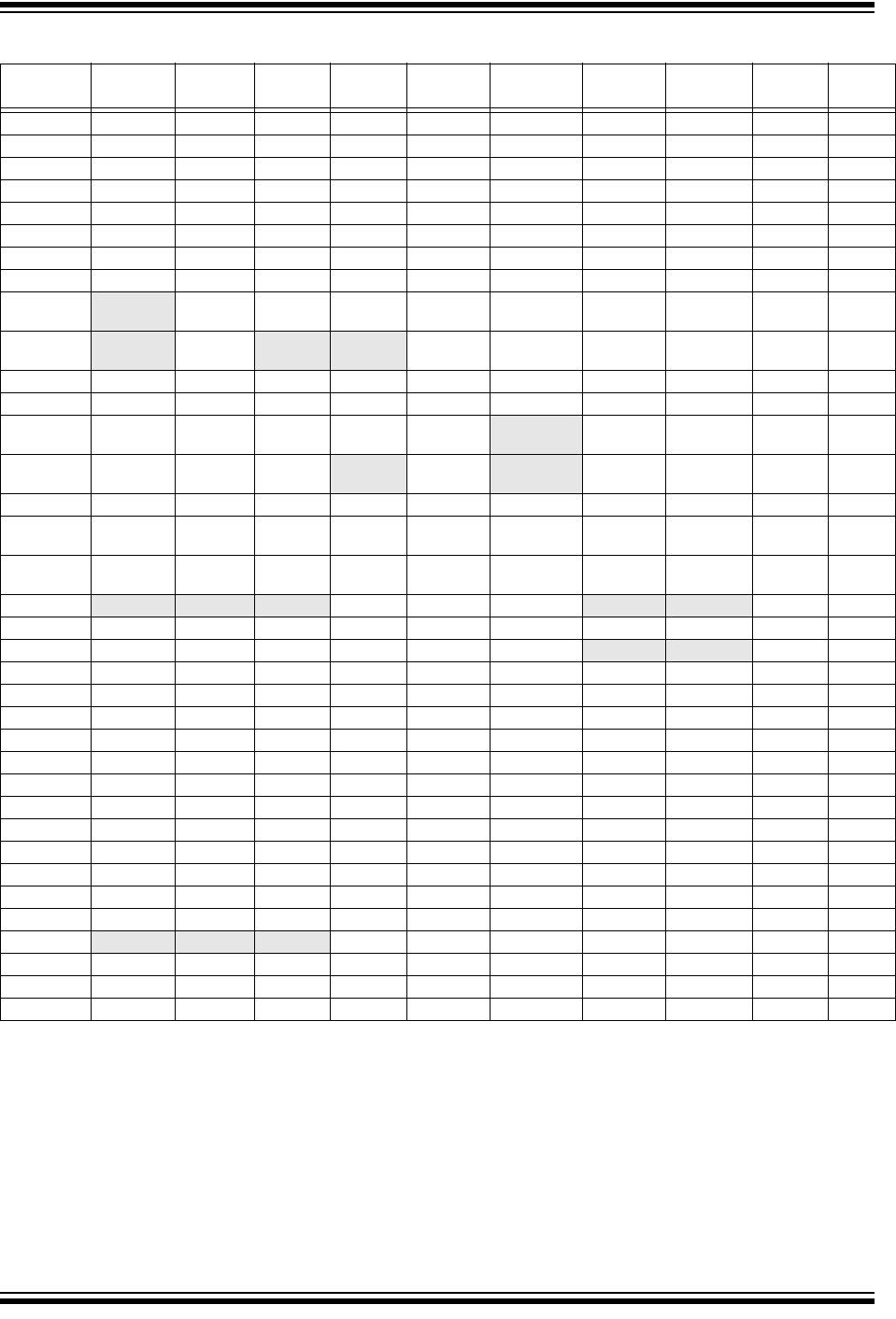
TABLE 6-2: REGISTER FILE SUMMARY (PIC18F2480/2580/4480/4580) (CONTINUED)
File Name Bit 7 Bit 6 Bit 5 Bit 4 Bit 3 Bit 2 Bit 1 Bit 0
Value on
POR, BOR
Details on
Page:
Legend: x = unknown, u = unchanged, - = unimplemented, q = value depends on condition
Note 1: Bit 21 of the PC is only available in Test mode and Serial Programming modes.
2: The SBOREN bit is only available when CONFIG2L<1:0> = 01; otherwise, it is disabled and reads as ‘0’. See Section 5.4 “Brown-out Reset (BOR)”.
3: These registers and/or bits are not implemented on PIC18F2X80 devices and are read as ‘0’. Reset values are shown for PIC18F4X80 devices;
individual unimplemented bits should be interpreted as ‘—’.
4: The PLLEN bit is only available in specific oscillator configuration; otherwise, it is disabled and reads as ‘0’. See Section 3.6.4 “PLL in INTOSC
Modes”.
5: The RE3 bit is only available when Master Clear Reset is disabled (CONFIG3H<7> = 0); otherwise, RE3 reads as ‘0’. This bit is read-only.
6: RA6/RA7 and their associated latch and direction bits are individually configured as port pins based on various primary oscillator modes. When
disabled, these bits read as ‘0’.
7: CAN bits have multiple functions depending on the selected mode of the CAN module.
8: This register reads all ‘0’s until the ECAN™ technology is set up in Mode 1 or Mode 2.
9: These registers are available on PIC18F4X80 devices only.