
Datasheet


Table Of Contents
- Power-Managed Modes:
- Flexible Oscillator Structure:
- Special Microcontroller Features:
- Peripheral Highlights:
- ECAN Technology Module Features:
- Pin Diagrams
- Pin Diagrams (Continued)
- Table of Contents
- Most Current Data Sheet
- Errata
- Customer Notification System
- 1.0 Device Overview
- 2.0 Guidelines for Getting Started with PIC18F Microcontrollers
- 3.0 Oscillator Configurations
- 4.0 Power-Managed Modes
- 5.0 Reset
- 5.1 RCON Register
- 5.2 Master Clear Reset (MCLR)
- 5.3 Power-on Reset (POR)
- 5.4 Brown-out Reset (BOR)
- 5.5 Device Reset Timers
- 5.5.1 Power-up Timer (PWRT)
- 5.5.2 Oscillator Start-up Timer (OST)
- 5.5.3 PLL Lock Time-out
- 5.5.4 Time-out Sequence
- TABLE 5-2: Time-out in Various Situations
- FIGURE 5-3: Time-out Sequence on Power-up (MCLR Tied to Vdd, Vdd Rise < Tpwrt)
- FIGURE 5-4: Time-out Sequence on Power-up (MCLR Not Tied to Vdd): Case 1
- FIGURE 5-5: Time-out Sequence on Power-up (MCLR Not Tied to Vdd): Case 2
- FIGURE 5-6: Slow Rise Time (MCLR Tied to Vdd, Vdd Rise > Tpwrt)
- FIGURE 5-7: Time-out Sequence on POR w/PLL Enabled (MCLR Tied to Vdd)
- 5.6 Reset State of Registers
- 6.0 Memory Organization
- 6.1 Program Memory Organization
- 6.2 PIC18 Instruction Cycle
- 6.3 Data Memory Organization
- 6.4 Data Addressing Modes
- 6.5 Program Memory and the Extended Instruction Set
- 6.6 Data Memory and the Extended Instruction Set
- 7.0 Flash Program Memory
- 7.1 Table Reads and Table Writes
- 7.2 Control Registers
- 7.3 Reading the Flash Program Memory
- 7.4 Erasing Flash Program Memory
- 7.5 Writing to Flash Program Memory
- 7.6 Flash Program Operation During Code Protection
- 8.0 Data EEPROM Memory
- 9.0 8 x 8 Hardware Multiplier
- 9.1 Introduction
- 9.2 Operation
- EXAMPLE 9-1: 8 x 8 Unsigned Multiply Routine
- EXAMPLE 9-2: 8 x 8 Signed Multiply Routine
- TABLE 9-1: Performance Comparison for Various Multiply Operations
- EQUATION 9-1: 16 x 16 Unsigned Multiplication Algorithm
- EXAMPLE 9-3: 16 x 16 Unsigned Multiply Routine
- EQUATION 9-2: 16 x 16 Signed Multiplication Algorithm
- EXAMPLE 9-4: 16 x 16 Signed Multiply Routine
- 10.0 Interrupts
- 11.0 I/O Ports
- 12.0 Timer0 Module
- 13.0 Timer1 Module
- 14.0 Timer2 Module
- 15.0 Timer3 Module
- 16.0 Capture/Compare/PWM (CCP) Modules
- Register 16-1: CCP1CON: Capture/Compare/PWM Control Register
- 16.1 CCP Module Configuration
- 16.2 Capture Mode
- 16.3 Compare Mode
- 16.4 PWM Mode
- 17.0 Enhanced Capture/Compare/PWM (ECCP) Module
- Register 17-1: ECCP1CON Register (ECCP1 module, PIC18F4480/4580 Devices)
- 17.1 ECCP Outputs and Configuration
- 17.2 Capture and Compare Modes
- 17.3 Standard PWM Mode
- 17.4 Enhanced PWM Mode
- 18.0 Master Synchronous Serial Port (MSSP) Module
- 18.1 Master SSP (MSSP) Module Overview
- 18.2 Control Registers
- 18.3 SPI Mode
- 18.4 I2C Mode
- FIGURE 18-7: MSSP Block Diagram (I2C™ Mode)
- 18.4.1 Registers
- 18.4.2 Operation
- 18.4.3 Slave Mode
- 18.4.4 Clock Stretching
- 18.4.5 General Call Address Support
- 18.4.6 Master Mode
- 18.4.7 Baud Rate
- 18.4.8 I2C Master Mode Start Condition Timing
- 18.4.9 I2C Master Mode Repeated Start Condition Timing
- 18.4.10 I2C Master Mode Transmission
- 18.4.11 I2C Master Mode Reception
- 18.4.12 Acknowledge Sequence Timing
- 18.4.13 Stop Condition Timing
- 18.4.14 Sleep Operation
- 18.4.15 Effect of a Reset
- 18.4.16 Multi-Master Mode
- 18.4.17 Multi-Master Communication, Bus Collision and Bus Arbitration
- FIGURE 18-25: Bus Collision Timing for Transmit and Acknowledge
- FIGURE 18-26: Bus Collision During Start Condition (SDA Only)
- FIGURE 18-27: Bus Collision During Start Condition (SCL = 0)
- FIGURE 18-28: BRG Reset Due to SDA Arbitration During Start Condition
- FIGURE 18-29: Bus Collision During a Repeated Start Condition (Case 1)
- FIGURE 18-30: Bus Collision During Repeated Start Condition (Case 2)
- FIGURE 18-31: Bus Collision During a Stop Condition (Case 1)
- FIGURE 18-32: Bus Collision During a Stop Condition (Case 2)
- 19.0 Enhanced Universal Synchronous Receiver Transmitter (EUSART)
- Register 19-1: TXSTA: Transmit Status And Control Register
- Register 19-2: RCSTA: Receive Status And Control Register
- Register 19-3: BAUDCON: Baud Rate Control Register
- 19.1 Baud Rate Generator (BRG)
- 19.2 EUSART Asynchronous Mode
- 19.3 EUSART Synchronous Master Mode
- 19.4 EUSART Synchronous Slave Mode
- 20.0 10-Bit Analog-to-Digital Converter (A/D) Module
- Register 20-1: ADCON0: A/D Control Register 0
- Register 20-2: ADCON1: A/D Control Register 1
- Register 20-3: ADCON2: A/D Control Register 2
- FIGURE 20-1: A/D Block Diagram
- FIGURE 20-2: Analog Input Model
- 20.1 A/D Acquisition Requirements
- 20.2 Selecting and Configuring Automatic Acquisition Time
- 20.3 Selecting the A/D Conversion Clock
- 20.4 Operation in Power-Managed Modes
- 20.5 Configuring Analog Port Pins
- 20.6 A/D Conversions
- 20.7 Use of the CCP1 Trigger
- 21.0 Comparator Module
- Register 21-1: CMCON: Comparator Control Register
- 21.1 Comparator Configuration
- 21.2 Comparator Operation
- 21.3 Comparator Reference
- 21.4 Comparator Response Time
- 21.5 Comparator Outputs
- 21.6 Comparator Interrupts
- 21.7 Comparator Operation During Sleep
- 21.8 Effects of a Reset
- 21.9 Analog Input Connection Considerations
- 22.0 Comparator Voltage Reference Module
- 23.0 High/Low-Voltage Detect (HLVD)
- 24.0 ECAN Module
- 24.1 Module Overview
- 24.2 CAN Module Registers
- 24.2.1 CAN Control and Status Registers
- Register 24-1: CANCON: CAN Control Register
- Register 24-2: CANSTAT: CAN Status Register
- EXAMPLE 24-1: Changing to Configuration Mode
- EXAMPLE 24-2: WIN and ICODE Bits Usage in Interrupt Service Routine to Access TX/RX Buffers
- EXAMPLE 24-2: WIN and ICODE Bits Usage in Interrupt Service Routine to Access TX/RX Buffers (Continued)
- Register 24-3: ECANCON: Enhanced CAN Control Register
- Register 24-4: COMSTAT: Communication Status Register
- 24.2.2 Dedicated CAN Transmit Buffer Registers
- Register 24-5: TXBnCON: Transmit Buffer n Control Registers [0 £ n £ 2]
- Register 24-6: TXBnSIDH: Transmit Buffer n Standard Identifier Registers, High Byte [0 £ n £ 2]
- Register 24-7: TXBnSIDL: Transmit Buffer n Standard Identifier Registers, Low Byte [0 £ n £ 2]
- Register 24-8: TXBnEIDH: Transmit Buffer n Extended Identifier Registers, High Byte [0 £ n £ 2]
- Register 24-9: TXBnEIDL: Transmit Buffer n Extended Identifier Registers, Low Byte [0 £ n £ 2]
- Register 24-10: TXBnDm: Transmit Buffer n Data Field Byte m Registers [0 £ n £ 2, 0 £ m £ 7]
- Register 24-11: TXBnDLC: Transmit Buffer n Data Length Code Registers [0 £ n £ 2]
- Register 24-12: TXERRCNT: Transmit Error Count Register
- EXAMPLE 24-3: Transmitting a CAN Message Using Banked Method
- EXAMPLE 24-4: Transmitting a CAN Message Using WIN Bits
- 24.2.3 Dedicated CAN Receive Buffer Registers
- Register 24-13: RXB0CON: Receive Buffer 0 Control Register
- Register 24-14: RXB1CON: Receive Buffer 1 Control Register
- Register 24-15: RXBnSIDH: Receive Buffer n Standard Identifier Registers, High Byte [0 £ n £ 1]
- Register 24-16: RXBnSIDL: Receive Buffer n Standard Identifier Registers, Low Byte [0 £ n £ 1]
- Register 24-17: RXBnEIDH: Receive Buffer n Extended Identifier Registers, High Byte [0 £ n £ 1]
- Register 24-18: RXBnEIDL: Receive Buffer n Extended Identifier Registers, Low Byte [0 £ n £ 1]
- Register 24-19: RXBnDLC: Receive Buffer n Data Length Code Registers [0 £ n £ 1]
- Register 24-20: RXBnDm: Receive Buffer n Data Field Byte m Registers [0 £ n £ 1, 0 £ m £ 7]
- Register 24-21: RXERRCNT: Receive Error Count Register
- EXAMPLE 24-5: Reading a CAN Message
- Register 24-22: BnCON: TX/RX Buffer n Control Registers in Receive Mode [0 £ n £ 5, TXnEN (bsel0
) = 0](1) - Register 24-23: BnCON: TX/RX Buffer n Control Registers in Transmit Mode [0 £ n £ 5, TXnEN (bsel0
) = 1](1) - Register 24-24: BnSIDH: TX/RX Buffer n Standard Identifier Registers, High Byte in Receive Mode [0 £ n £ 5, TXnEN (BSEL0
) = 0](1) - Register 24-25: BnSIDH: TX/RX Buffer n Standard Identifier Registers, High Byte in Transmit Mode [0 £ n £ 5, TXnEN (BSEL0
) = 1](1) - Register 24-26: BnSIDL: TX/RX Buffer n Standard Identifier Registers, Low Byte in Receive Mode [0 £ n £ 5, TXnEN (bsel0
) = 0](1) - Register 24-27: BnSIDL: TX/RX Buffer n Standard Identifier Registers, Low Byte in Receive Mode [0 £ n £ 5, TXnEN (bsel0
) = 1](1) - Register 24-28: BnEIDH: TX/RX Buffer n Extended Identifier Registers, High Byte in Receive Mode [0 £ n £ 5, TXnEN (BSEL0
) = 0](1) - Register 24-29: BnEIDH: TX/RX Buffer n Extended Identifier Registers, High Byte in Transmit Mode [0 £ n £ 5, TXnEN (BSEL0
) = 1](1) - Register 24-30: BnEIDL: TX/RX Buffer n Extended Identifier Registers, Low Byte in Receive Mode [0 £ n £ 5, TXnEN (BSEL
) = 0](1) - Register 24-31: BnEIDL: TX/RX Buffer n Extended Identifier Registers, Low Byte in Receive Mode [0 £ n £ 5, TXnEN (BSEL
) = 1](1) - Register 24-32: BnDm: TX/RX Buffer n Data Field Byte m Registers in Receive Mode [0 £ n £ 5, 0 £ m £ 7, TXnEN (BSEL
) = 0](1) - Register 24-33: BnDm: TX/RX Buffer n Data Field Byte m Registers in Transmit Mode [0 £ n £ 5, 0 £ m £ 7, TXnEN (BSEL
) = 1](1) - Register 24-34: BnDLC: TX/RX Buffer n Data Length Code Registers in Receive Mode [0 £ n £ 5, TXnEN (BSEL
) = 0](1) - Register 24-35: BnDLC: TX/RX Buffer n Data Length Code Registers in Transmit Mode [0 £ n £ 5, TXnEN (BSEL
) = 1](1) - Register 24-36: BSEL0: Buffer Select Register 0(1)
- Register 24-37: RXFnSIDH: Receive Acceptance Filter n Standard Identifier Filter Registers, High Byte [0 £ n £ 15](1)
- Register 24-38: RXFnSIDL: Receive Acceptance Filter n Standard Identifier Filter Registers, Low Byte [0 £ n £ 15](1)
- Register 24-39: RXFnEIDH: Receive Acceptance Filter n Extended Identifier Registers, High Byte [0 £ n £ 15](1)
- Register 24-40: RXFnEIDL: Receive Acceptance Filter n Extended Identifier Registers, Low Byte [0 £ n £ 15](1)
- Register 24-41: RXMnSIDH: Receive Acceptance Mask n Standard Identifier Mask Registers, High Byte [0 £ n £ 1]
- Register 24-42: RXMnSIDL: Receive Acceptance Mask n Standard Identifier Mask Registers, Low Byte [0 £ n £ 1]
- Register 24-43: RXMnEIDH: Receive Acceptance Mask n Extended Identifier Mask Registers, High Byte [0 £ n £ 1]
- Register 24-44: RXMnEIDL: Receive Acceptance Mask n Extended Identifier Mask Registers, Low Byte [0 £ n £ 1]
- Register 24-45: RXFCONn: Receive Filter Control Register n [0 £ n £ 1](1)
- Register 24-46: SDFLC: Standard Data Bytes Filter Length Count Register(1)
- Register 24-47: RXFBCONn: Receive Filter Buffer Control Register n(1)
- Register 24-48: MSEL0: Mask Select Register 0(1)
- Register 24-49: MSEL1: Mask Select Register 1(1)
- Register 24-50: MSEL2: Mask Select Register 2(1)
- Register 24-51: MSEL3: Mask Select Register 3(1)
- 24.2.4 CAN Baud Rate Registers
- 24.2.5 CAN Module I/O Control Register
- 24.2.6 CAN Interrupt Registers
- Register 24-56: PIR3: Peripheral Interrupt Request (Flag) Register 3
- Register 24-57: PIE3: Peripheral Interrupt Enable Register 3
- Register 24-58: IPR3: Peripheral Interrupt Priority Register 3
- Register 24-59: TXBIE: Transmit Buffers Interrupt Enable Register(1)
- Register 24-60: BIE0: Buffer Interrupt Enable Register 0(1)
- TABLE 24-1: Can Controller Register Map
- TABLE 24-1: Can Controller Register Map (continued)
- 24.2.1 CAN Control and Status Registers
- 24.3 CAN Modes of Operation
- 24.4 CAN Module Functional Modes
- 24.5 CAN Message Buffers
- 24.6 CAN Message Transmission
- 24.7 Message Reception
- 24.8 Message Acceptance Filters and Masks
- 24.9 Baud Rate Setting
- EQUATION 24-1:
- EQUATION 24-2:
- EQUATION 24-3:
- FIGURE 24-4: Bit Time Partitioning
- 24.9.1 External Clock, Internal Clock and Measurable Jitter in HS-PLL Based Oscillators
- 24.9.2 Time Quanta
- 24.9.3 Synchronization Segment
- 24.9.4 Propagation Segment
- 24.9.5 Phase Buffer Segments
- 24.9.6 Sample Point
- 24.9.7 Information Processing Time
- 24.10 Synchronization
- 24.11 Programming Time Segments
- 24.12 Oscillator Tolerance
- 24.13 Bit Timing Configuration Registers
- 24.14 Error Detection
- 24.15 CAN Interrupts
- 25.0 Special Features of the CPU
- 25.1 Configuration Bits
- TABLE 25-1: Configuration Bits and Device IDs
- Register 25-1: CONFIG1H: Configuration Register 1 High (Byte Address 300001h)
- Register 25-2: CONFIG2L: Configuration Register 2 Low (Byte Address 300002h)
- Register 25-3: CONFIG2H: Configuration Register 2 High (Byte Address 300003h)
- Register 25-4: CONFIG3H: Configuration Register 3 High (Byte Address 300005h)
- Register 25-5: CONFIG4L: Configuration Register 4 Low (Byte Address 300006h)
- Register 25-6: CONFIG5L: Configuration Register 5 Low (Byte Address 300008h)
- Register 25-7: CONFIG5H: Configuration Register 5 High (Byte Address 300009h)
- Register 25-8: CONFIG6L: Configuration Register 6 Low (Byte Address 30000Ah)
- Register 25-9: CONFIG6H: Configuration Register 6 High (Byte Address 30000Bh)
- Register 25-10: CONFIG7L: Configuration Register 7 Low (Byte Address 30000Ch)
- Register 25-11: CONFIG7H: Configuration Register 7 High (Byte Address 30000Dh)
- Register 25-12: DEVID1: Device ID Register 1 for PIC18F2480/2580/4480/4580
- Register 25-13: DEVID2: Device ID Register 2 for PIC18F2480/2580/4480/4580
- 25.2 Watchdog Timer (WDT)
- 25.3 Two-Speed Start-up
- 25.4 Fail-Safe Clock Monitor
- 25.5 Program Verification and Code Protection
- 25.6 ID Locations
- 25.7 In-Circuit Serial Programming
- 25.8 In-Circuit Debugger
- 25.9 Single-Supply ICSP Programming
- 25.1 Configuration Bits
- 26.0 Instruction Set Summary
- 26.1 Standard Instruction Set
- 26.2 Extended Instruction Set
- 27.0 Development Support
- 27.1 MPLAB Integrated Development Environment Software
- 27.2 MPLAB C Compilers for Various Device Families
- 27.3 HI-TECH C for Various Device Families
- 27.4 MPASM Assembler
- 27.5 MPLINK Object Linker/ MPLIB Object Librarian
- 27.6 MPLAB Assembler, Linker and Librarian for Various Device Families
- 27.7 MPLAB SIM Software Simulator
- 27.8 MPLAB REAL ICE In-Circuit Emulator System
- 27.9 MPLAB ICD 3 In-Circuit Debugger System
- 27.10 PICkit 3 In-Circuit Debugger/ Programmer and PICkit 3 Debug Express
- 27.11 PICkit 2 Development Programmer/Debugger and PICkit 2 Debug Express
- 27.12 MPLAB PM3 Device Programmer
- 27.13 Demonstration/Development Boards, Evaluation Kits, and Starter Kits
- 28.0 Electrical Characteristics
- Absolute Maximum Ratings (†)
- 28.1 DC Characteristics: Supply Voltage PIC18F2480/2580/4480/4580 (Industrial, Extended) PIC18LF2480/2580/4480/4580 (Industrial)
- 28.2 DC Characteristics: Power-Down and Supply Current PIC18F2480/2580/4480/4580 (Industrial, Extended) PIC18LF2480/2580/4480/4580 (Industrial)
- 28.3 DC Characteristics: PIC18F2480/2580/4480/4580 (Industrial) PIC18LF2480/2580/4480/4580 (Industrial)
- 28.4 AC (Timing) Characteristics
- 28.4.1 Timing Parameter Symbology
- 28.4.2 Timing Conditions
- 28.4.3 Timing Diagrams and Specifications
- FIGURE 28-5: External Clock Timing (All Modes Except PLL)
- TABLE 28-6: External Clock Timing Requirements
- TABLE 28-7: PLL Clock Timing Specifications (Vdd = 4.2V to 5.5V)
- TABLE 28-8: AC Characteristics: Internal RC Accuracy PIC18F2480/2580/4480/4580 (Industrial) PIC18LF2480/2580/4480/4580 (Industrial)
- FIGURE 28-6: CLKO and I/O Timing
- TABLE 28-9: CLKO and I/O Timing Requirements
- FIGURE 28-7: Reset, Watchdog Timer, Oscillator Start-up Timer and Power-up Timer Timing
- FIGURE 28-8: Brown-out Reset Timing
- TABLE 28-10: Reset, Watchdog Timer, Oscillator Start-up Timer, Power-up Timer and Brown-out Reset Requirements
- FIGURE 28-9: Timer0 and Timer1 External Clock Timings
- TABLE 28-11: Timer0 and Timer1 External Clock Requirements
- FIGURE 28-10: Capture/Compare/PWM Timings (All CCP Modules)
- TABLE 28-12: Capture/Compare/PWM Requirements (All CCP Modules)
- FIGURE 28-11: Parallel Slave Port Timing (PIC18F4480/4580)
- TABLE 28-13: Parallel Slave Port Requirements (PIC18F4480/4580)
- FIGURE 28-12: Example SPI Master Mode Timing (CKE = 0)
- TABLE 28-14: Example SPI Mode Requirements (Master Mode, CKE = 0)
- FIGURE 28-13: Example SPI Master Mode Timing (CKE = 1)
- TABLE 28-15: Example SPI Mode Requirements (Master Mode, CKE = 1)
- FIGURE 28-14: Example SPI Slave Mode Timing (CKE = 0)
- TABLE 28-16: Example SPI Mode Requirements (Slave Mode Timing, CKE = 0)
- FIGURE 28-15: Example SPI Slave Mode Timing (CKE = 1)
- TABLE 28-17: Example SPI Slave Mode Requirements (CKE = 1)
- FIGURE 28-16: I2C™ Bus Start/Stop Bits Timing
- TABLE 28-18: I2C™ Bus Start/Stop Bits Requirements (Slave Mode)
- FIGURE 28-17: I2C™ Bus Data Timing
- TABLE 28-19: I2C™ Bus Data Requirements (Slave Mode)
- FIGURE 28-18: Master SSP I2C™ Bus Start/Stop Bits Timing Waveforms
- TABLE 28-20: Master SSP I2C™ Bus Start/Stop Bits Requirements
- FIGURE 28-19: Master SSP I2C™ Bus Data Timing
- TABLE 28-21: Master SSP I2c™ Bus Data Requirements
- FIGURE 28-20: EUSART Synchronous Transmission (Master/Slave) Timing
- TABLE 28-22: EUSART Synchronous Transmission Requirements
- FIGURE 28-21: EUSART Synchronous Receive (Master/Slave) Timing
- TABLE 28-23: EUSART Synchronous Receive Requirements
- TABLE 28-24: A/D Converter Characteristics: PIC18F2480/2580/4480/4580 (Industrial) PIC18LF2480/2580/4480/4580 (Industrial)
- FIGURE 28-22: A/D Conversion Timing
- TABLE 28-25: A/D Conversion Requirements
- 29.0 Packaging Information
- Appendix A: Revision History
- Appendix B: Device Differences
- Appendix C: Conversion Considerations
- Appendix D: Migration from Baseline to Enhanced Devices
- Appendix E: Migration From Mid-Range to Enhanced Devices
- Appendix F: Migration From High-End to Enhanced Devices
- INDEX
- The Microchip Web Site
- Customer Change Notification Service
- Customer Support
- Reader Response
- PIC18F2480/2580/4480/4580 Product Identification System
- Worldwide Sales and Service
© 2009 Microchip Technology Inc. DS39637D-page 355
PIC18F2480/2580/4480/4580
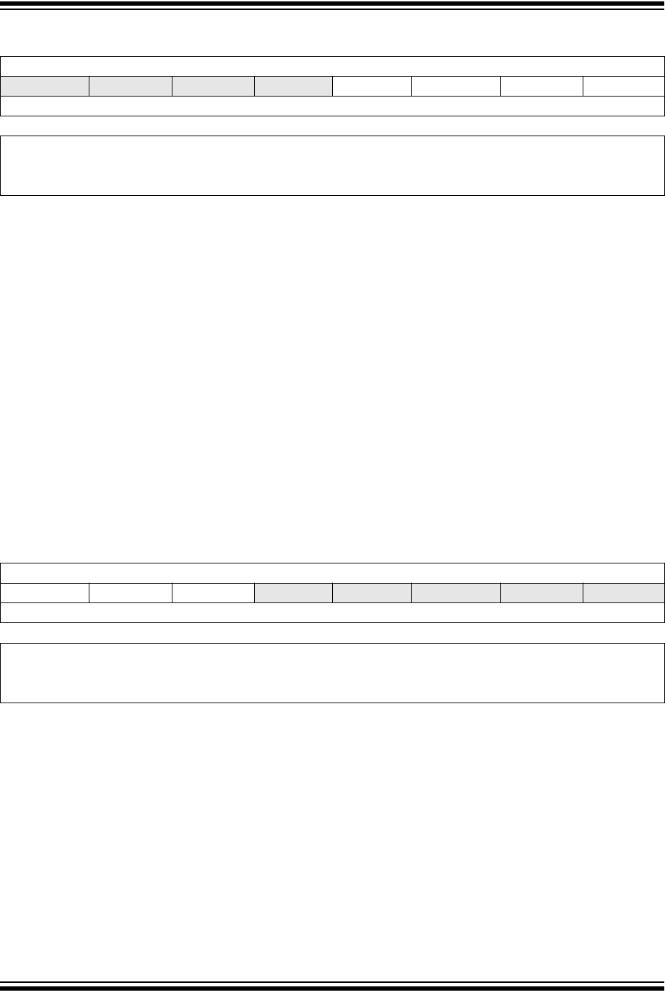
REGISTER 25-8: CONFIG6L: CONFIGURATION REGISTER 6 LOW (BYTE ADDRESS 30000Ah)
U-0 U-0 U-0 U-0 R/C-1 R/C-1 R/C-1 R/C-1
— — — —WRT3
(1)
WRT2
(1)
WRT1 WRT0
bit 7 bit 0
Legend:
R = Readable bit C = Clearable bit U = Unimplemented bit, read as ‘0’
-n = Value when device is unprogrammed u = Unchanged from programmed state
bit 7-4 Unimplemented: Read as ‘0’
bit 3 WRT3: Write Protection bit
(1)
1 = Block 3 (006000-007FFFh) not write-protected
0 = Block 3 (006000-007FFFh) write-protected
bit 2 WRT2: Write Protection bit
(1)
1 = Block 2 (004000-005FFFh) not write-protected
0 = Block 2 (004000-005FFFh) write-protected
bit 1 WRT1: Write Protection bit
1 = Block 1 (002000-003FFFh) not write-protected
0 = Block 1 (002000-003FFFh) write-protected
bit 0 WRT0: Write Protection bit
1 = Block 0 (000800-001FFFh) not write-protected
0 = Block 0 (000800-001FFFh) write-protected
Note 1: Unimplemented in PIC18FX480 devices; maintain this bit set.
REGISTER 25-9: CONFIG6H: CONFIGURATION REGISTER 6 HIGH (BYTE ADDRESS 30000Bh)
R/C-1 R/C-1 R-1 U-0 U-0 U-0 U-0 U-0
WRTD WRTB WRTC
(1)
— — — — —
bit 7 bit 0
Legend:
R = Readable bit C = Clearable bit U = Unimplemented bit, read as ‘0’
-n = Value when device is unprogrammed u = Unchanged from programmed state
bit 7 WRTD: Data EEPROM Write Protection bit
1 = Data EEPROM not write-protected
0 = Data EEPROM write-protected
bit 6 WRTB: Boot Block Write Protection bit
1 = Boot Block (000000-0007FFh) not write-protected
0 = Boot Block (000000-0007FFh) write-protected
bit 5 WRTC: Configuration Register Write Protection bit
(1)
1 = Configuration registers (300000-3000FFh) not write-protected
0 = Configuration registers (300000-3000FFh) write-protected
bit 4-0 Unimplemented: Read as ‘0’
Note 1: This bit is read-only in normal execution mode; it can be written only in Program mode.