
Datasheet


Table Of Contents
- Power-Managed Modes:
- Flexible Oscillator Structure:
- Special Microcontroller Features:
- Peripheral Highlights:
- ECAN Technology Module Features:
- Pin Diagrams
- Pin Diagrams (Continued)
- Table of Contents
- Most Current Data Sheet
- Errata
- Customer Notification System
- 1.0 Device Overview
- 2.0 Guidelines for Getting Started with PIC18F Microcontrollers
- 3.0 Oscillator Configurations
- 4.0 Power-Managed Modes
- 5.0 Reset
- 5.1 RCON Register
- 5.2 Master Clear Reset (MCLR)
- 5.3 Power-on Reset (POR)
- 5.4 Brown-out Reset (BOR)
- 5.5 Device Reset Timers
- 5.5.1 Power-up Timer (PWRT)
- 5.5.2 Oscillator Start-up Timer (OST)
- 5.5.3 PLL Lock Time-out
- 5.5.4 Time-out Sequence
- TABLE 5-2: Time-out in Various Situations
- FIGURE 5-3: Time-out Sequence on Power-up (MCLR Tied to Vdd, Vdd Rise < Tpwrt)
- FIGURE 5-4: Time-out Sequence on Power-up (MCLR Not Tied to Vdd): Case 1
- FIGURE 5-5: Time-out Sequence on Power-up (MCLR Not Tied to Vdd): Case 2
- FIGURE 5-6: Slow Rise Time (MCLR Tied to Vdd, Vdd Rise > Tpwrt)
- FIGURE 5-7: Time-out Sequence on POR w/PLL Enabled (MCLR Tied to Vdd)
- 5.6 Reset State of Registers
- 6.0 Memory Organization
- 6.1 Program Memory Organization
- 6.2 PIC18 Instruction Cycle
- 6.3 Data Memory Organization
- 6.4 Data Addressing Modes
- 6.5 Program Memory and the Extended Instruction Set
- 6.6 Data Memory and the Extended Instruction Set
- 7.0 Flash Program Memory
- 7.1 Table Reads and Table Writes
- 7.2 Control Registers
- 7.3 Reading the Flash Program Memory
- 7.4 Erasing Flash Program Memory
- 7.5 Writing to Flash Program Memory
- 7.6 Flash Program Operation During Code Protection
- 8.0 Data EEPROM Memory
- 9.0 8 x 8 Hardware Multiplier
- 9.1 Introduction
- 9.2 Operation
- EXAMPLE 9-1: 8 x 8 Unsigned Multiply Routine
- EXAMPLE 9-2: 8 x 8 Signed Multiply Routine
- TABLE 9-1: Performance Comparison for Various Multiply Operations
- EQUATION 9-1: 16 x 16 Unsigned Multiplication Algorithm
- EXAMPLE 9-3: 16 x 16 Unsigned Multiply Routine
- EQUATION 9-2: 16 x 16 Signed Multiplication Algorithm
- EXAMPLE 9-4: 16 x 16 Signed Multiply Routine
- 10.0 Interrupts
- 11.0 I/O Ports
- 12.0 Timer0 Module
- 13.0 Timer1 Module
- 14.0 Timer2 Module
- 15.0 Timer3 Module
- 16.0 Capture/Compare/PWM (CCP) Modules
- Register 16-1: CCP1CON: Capture/Compare/PWM Control Register
- 16.1 CCP Module Configuration
- 16.2 Capture Mode
- 16.3 Compare Mode
- 16.4 PWM Mode
- 17.0 Enhanced Capture/Compare/PWM (ECCP) Module
- Register 17-1: ECCP1CON Register (ECCP1 module, PIC18F4480/4580 Devices)
- 17.1 ECCP Outputs and Configuration
- 17.2 Capture and Compare Modes
- 17.3 Standard PWM Mode
- 17.4 Enhanced PWM Mode
- 18.0 Master Synchronous Serial Port (MSSP) Module
- 18.1 Master SSP (MSSP) Module Overview
- 18.2 Control Registers
- 18.3 SPI Mode
- 18.4 I2C Mode
- FIGURE 18-7: MSSP Block Diagram (I2C™ Mode)
- 18.4.1 Registers
- 18.4.2 Operation
- 18.4.3 Slave Mode
- 18.4.4 Clock Stretching
- 18.4.5 General Call Address Support
- 18.4.6 Master Mode
- 18.4.7 Baud Rate
- 18.4.8 I2C Master Mode Start Condition Timing
- 18.4.9 I2C Master Mode Repeated Start Condition Timing
- 18.4.10 I2C Master Mode Transmission
- 18.4.11 I2C Master Mode Reception
- 18.4.12 Acknowledge Sequence Timing
- 18.4.13 Stop Condition Timing
- 18.4.14 Sleep Operation
- 18.4.15 Effect of a Reset
- 18.4.16 Multi-Master Mode
- 18.4.17 Multi-Master Communication, Bus Collision and Bus Arbitration
- FIGURE 18-25: Bus Collision Timing for Transmit and Acknowledge
- FIGURE 18-26: Bus Collision During Start Condition (SDA Only)
- FIGURE 18-27: Bus Collision During Start Condition (SCL = 0)
- FIGURE 18-28: BRG Reset Due to SDA Arbitration During Start Condition
- FIGURE 18-29: Bus Collision During a Repeated Start Condition (Case 1)
- FIGURE 18-30: Bus Collision During Repeated Start Condition (Case 2)
- FIGURE 18-31: Bus Collision During a Stop Condition (Case 1)
- FIGURE 18-32: Bus Collision During a Stop Condition (Case 2)
- 19.0 Enhanced Universal Synchronous Receiver Transmitter (EUSART)
- Register 19-1: TXSTA: Transmit Status And Control Register
- Register 19-2: RCSTA: Receive Status And Control Register
- Register 19-3: BAUDCON: Baud Rate Control Register
- 19.1 Baud Rate Generator (BRG)
- 19.2 EUSART Asynchronous Mode
- 19.3 EUSART Synchronous Master Mode
- 19.4 EUSART Synchronous Slave Mode
- 20.0 10-Bit Analog-to-Digital Converter (A/D) Module
- Register 20-1: ADCON0: A/D Control Register 0
- Register 20-2: ADCON1: A/D Control Register 1
- Register 20-3: ADCON2: A/D Control Register 2
- FIGURE 20-1: A/D Block Diagram
- FIGURE 20-2: Analog Input Model
- 20.1 A/D Acquisition Requirements
- 20.2 Selecting and Configuring Automatic Acquisition Time
- 20.3 Selecting the A/D Conversion Clock
- 20.4 Operation in Power-Managed Modes
- 20.5 Configuring Analog Port Pins
- 20.6 A/D Conversions
- 20.7 Use of the CCP1 Trigger
- 21.0 Comparator Module
- Register 21-1: CMCON: Comparator Control Register
- 21.1 Comparator Configuration
- 21.2 Comparator Operation
- 21.3 Comparator Reference
- 21.4 Comparator Response Time
- 21.5 Comparator Outputs
- 21.6 Comparator Interrupts
- 21.7 Comparator Operation During Sleep
- 21.8 Effects of a Reset
- 21.9 Analog Input Connection Considerations
- 22.0 Comparator Voltage Reference Module
- 23.0 High/Low-Voltage Detect (HLVD)
- 24.0 ECAN Module
- 24.1 Module Overview
- 24.2 CAN Module Registers
- 24.2.1 CAN Control and Status Registers
- Register 24-1: CANCON: CAN Control Register
- Register 24-2: CANSTAT: CAN Status Register
- EXAMPLE 24-1: Changing to Configuration Mode
- EXAMPLE 24-2: WIN and ICODE Bits Usage in Interrupt Service Routine to Access TX/RX Buffers
- EXAMPLE 24-2: WIN and ICODE Bits Usage in Interrupt Service Routine to Access TX/RX Buffers (Continued)
- Register 24-3: ECANCON: Enhanced CAN Control Register
- Register 24-4: COMSTAT: Communication Status Register
- 24.2.2 Dedicated CAN Transmit Buffer Registers
- Register 24-5: TXBnCON: Transmit Buffer n Control Registers [0 £ n £ 2]
- Register 24-6: TXBnSIDH: Transmit Buffer n Standard Identifier Registers, High Byte [0 £ n £ 2]
- Register 24-7: TXBnSIDL: Transmit Buffer n Standard Identifier Registers, Low Byte [0 £ n £ 2]
- Register 24-8: TXBnEIDH: Transmit Buffer n Extended Identifier Registers, High Byte [0 £ n £ 2]
- Register 24-9: TXBnEIDL: Transmit Buffer n Extended Identifier Registers, Low Byte [0 £ n £ 2]
- Register 24-10: TXBnDm: Transmit Buffer n Data Field Byte m Registers [0 £ n £ 2, 0 £ m £ 7]
- Register 24-11: TXBnDLC: Transmit Buffer n Data Length Code Registers [0 £ n £ 2]
- Register 24-12: TXERRCNT: Transmit Error Count Register
- EXAMPLE 24-3: Transmitting a CAN Message Using Banked Method
- EXAMPLE 24-4: Transmitting a CAN Message Using WIN Bits
- 24.2.3 Dedicated CAN Receive Buffer Registers
- Register 24-13: RXB0CON: Receive Buffer 0 Control Register
- Register 24-14: RXB1CON: Receive Buffer 1 Control Register
- Register 24-15: RXBnSIDH: Receive Buffer n Standard Identifier Registers, High Byte [0 £ n £ 1]
- Register 24-16: RXBnSIDL: Receive Buffer n Standard Identifier Registers, Low Byte [0 £ n £ 1]
- Register 24-17: RXBnEIDH: Receive Buffer n Extended Identifier Registers, High Byte [0 £ n £ 1]
- Register 24-18: RXBnEIDL: Receive Buffer n Extended Identifier Registers, Low Byte [0 £ n £ 1]
- Register 24-19: RXBnDLC: Receive Buffer n Data Length Code Registers [0 £ n £ 1]
- Register 24-20: RXBnDm: Receive Buffer n Data Field Byte m Registers [0 £ n £ 1, 0 £ m £ 7]
- Register 24-21: RXERRCNT: Receive Error Count Register
- EXAMPLE 24-5: Reading a CAN Message
- Register 24-22: BnCON: TX/RX Buffer n Control Registers in Receive Mode [0 £ n £ 5, TXnEN (bsel0
) = 0](1) - Register 24-23: BnCON: TX/RX Buffer n Control Registers in Transmit Mode [0 £ n £ 5, TXnEN (bsel0
) = 1](1) - Register 24-24: BnSIDH: TX/RX Buffer n Standard Identifier Registers, High Byte in Receive Mode [0 £ n £ 5, TXnEN (BSEL0
) = 0](1) - Register 24-25: BnSIDH: TX/RX Buffer n Standard Identifier Registers, High Byte in Transmit Mode [0 £ n £ 5, TXnEN (BSEL0
) = 1](1) - Register 24-26: BnSIDL: TX/RX Buffer n Standard Identifier Registers, Low Byte in Receive Mode [0 £ n £ 5, TXnEN (bsel0
) = 0](1) - Register 24-27: BnSIDL: TX/RX Buffer n Standard Identifier Registers, Low Byte in Receive Mode [0 £ n £ 5, TXnEN (bsel0
) = 1](1) - Register 24-28: BnEIDH: TX/RX Buffer n Extended Identifier Registers, High Byte in Receive Mode [0 £ n £ 5, TXnEN (BSEL0
) = 0](1) - Register 24-29: BnEIDH: TX/RX Buffer n Extended Identifier Registers, High Byte in Transmit Mode [0 £ n £ 5, TXnEN (BSEL0
) = 1](1) - Register 24-30: BnEIDL: TX/RX Buffer n Extended Identifier Registers, Low Byte in Receive Mode [0 £ n £ 5, TXnEN (BSEL
) = 0](1) - Register 24-31: BnEIDL: TX/RX Buffer n Extended Identifier Registers, Low Byte in Receive Mode [0 £ n £ 5, TXnEN (BSEL
) = 1](1) - Register 24-32: BnDm: TX/RX Buffer n Data Field Byte m Registers in Receive Mode [0 £ n £ 5, 0 £ m £ 7, TXnEN (BSEL
) = 0](1) - Register 24-33: BnDm: TX/RX Buffer n Data Field Byte m Registers in Transmit Mode [0 £ n £ 5, 0 £ m £ 7, TXnEN (BSEL
) = 1](1) - Register 24-34: BnDLC: TX/RX Buffer n Data Length Code Registers in Receive Mode [0 £ n £ 5, TXnEN (BSEL
) = 0](1) - Register 24-35: BnDLC: TX/RX Buffer n Data Length Code Registers in Transmit Mode [0 £ n £ 5, TXnEN (BSEL
) = 1](1) - Register 24-36: BSEL0: Buffer Select Register 0(1)
- Register 24-37: RXFnSIDH: Receive Acceptance Filter n Standard Identifier Filter Registers, High Byte [0 £ n £ 15](1)
- Register 24-38: RXFnSIDL: Receive Acceptance Filter n Standard Identifier Filter Registers, Low Byte [0 £ n £ 15](1)
- Register 24-39: RXFnEIDH: Receive Acceptance Filter n Extended Identifier Registers, High Byte [0 £ n £ 15](1)
- Register 24-40: RXFnEIDL: Receive Acceptance Filter n Extended Identifier Registers, Low Byte [0 £ n £ 15](1)
- Register 24-41: RXMnSIDH: Receive Acceptance Mask n Standard Identifier Mask Registers, High Byte [0 £ n £ 1]
- Register 24-42: RXMnSIDL: Receive Acceptance Mask n Standard Identifier Mask Registers, Low Byte [0 £ n £ 1]
- Register 24-43: RXMnEIDH: Receive Acceptance Mask n Extended Identifier Mask Registers, High Byte [0 £ n £ 1]
- Register 24-44: RXMnEIDL: Receive Acceptance Mask n Extended Identifier Mask Registers, Low Byte [0 £ n £ 1]
- Register 24-45: RXFCONn: Receive Filter Control Register n [0 £ n £ 1](1)
- Register 24-46: SDFLC: Standard Data Bytes Filter Length Count Register(1)
- Register 24-47: RXFBCONn: Receive Filter Buffer Control Register n(1)
- Register 24-48: MSEL0: Mask Select Register 0(1)
- Register 24-49: MSEL1: Mask Select Register 1(1)
- Register 24-50: MSEL2: Mask Select Register 2(1)
- Register 24-51: MSEL3: Mask Select Register 3(1)
- 24.2.4 CAN Baud Rate Registers
- 24.2.5 CAN Module I/O Control Register
- 24.2.6 CAN Interrupt Registers
- Register 24-56: PIR3: Peripheral Interrupt Request (Flag) Register 3
- Register 24-57: PIE3: Peripheral Interrupt Enable Register 3
- Register 24-58: IPR3: Peripheral Interrupt Priority Register 3
- Register 24-59: TXBIE: Transmit Buffers Interrupt Enable Register(1)
- Register 24-60: BIE0: Buffer Interrupt Enable Register 0(1)
- TABLE 24-1: Can Controller Register Map
- TABLE 24-1: Can Controller Register Map (continued)
- 24.2.1 CAN Control and Status Registers
- 24.3 CAN Modes of Operation
- 24.4 CAN Module Functional Modes
- 24.5 CAN Message Buffers
- 24.6 CAN Message Transmission
- 24.7 Message Reception
- 24.8 Message Acceptance Filters and Masks
- 24.9 Baud Rate Setting
- EQUATION 24-1:
- EQUATION 24-2:
- EQUATION 24-3:
- FIGURE 24-4: Bit Time Partitioning
- 24.9.1 External Clock, Internal Clock and Measurable Jitter in HS-PLL Based Oscillators
- 24.9.2 Time Quanta
- 24.9.3 Synchronization Segment
- 24.9.4 Propagation Segment
- 24.9.5 Phase Buffer Segments
- 24.9.6 Sample Point
- 24.9.7 Information Processing Time
- 24.10 Synchronization
- 24.11 Programming Time Segments
- 24.12 Oscillator Tolerance
- 24.13 Bit Timing Configuration Registers
- 24.14 Error Detection
- 24.15 CAN Interrupts
- 25.0 Special Features of the CPU
- 25.1 Configuration Bits
- TABLE 25-1: Configuration Bits and Device IDs
- Register 25-1: CONFIG1H: Configuration Register 1 High (Byte Address 300001h)
- Register 25-2: CONFIG2L: Configuration Register 2 Low (Byte Address 300002h)
- Register 25-3: CONFIG2H: Configuration Register 2 High (Byte Address 300003h)
- Register 25-4: CONFIG3H: Configuration Register 3 High (Byte Address 300005h)
- Register 25-5: CONFIG4L: Configuration Register 4 Low (Byte Address 300006h)
- Register 25-6: CONFIG5L: Configuration Register 5 Low (Byte Address 300008h)
- Register 25-7: CONFIG5H: Configuration Register 5 High (Byte Address 300009h)
- Register 25-8: CONFIG6L: Configuration Register 6 Low (Byte Address 30000Ah)
- Register 25-9: CONFIG6H: Configuration Register 6 High (Byte Address 30000Bh)
- Register 25-10: CONFIG7L: Configuration Register 7 Low (Byte Address 30000Ch)
- Register 25-11: CONFIG7H: Configuration Register 7 High (Byte Address 30000Dh)
- Register 25-12: DEVID1: Device ID Register 1 for PIC18F2480/2580/4480/4580
- Register 25-13: DEVID2: Device ID Register 2 for PIC18F2480/2580/4480/4580
- 25.2 Watchdog Timer (WDT)
- 25.3 Two-Speed Start-up
- 25.4 Fail-Safe Clock Monitor
- 25.5 Program Verification and Code Protection
- 25.6 ID Locations
- 25.7 In-Circuit Serial Programming
- 25.8 In-Circuit Debugger
- 25.9 Single-Supply ICSP Programming
- 25.1 Configuration Bits
- 26.0 Instruction Set Summary
- 26.1 Standard Instruction Set
- 26.2 Extended Instruction Set
- 27.0 Development Support
- 27.1 MPLAB Integrated Development Environment Software
- 27.2 MPLAB C Compilers for Various Device Families
- 27.3 HI-TECH C for Various Device Families
- 27.4 MPASM Assembler
- 27.5 MPLINK Object Linker/ MPLIB Object Librarian
- 27.6 MPLAB Assembler, Linker and Librarian for Various Device Families
- 27.7 MPLAB SIM Software Simulator
- 27.8 MPLAB REAL ICE In-Circuit Emulator System
- 27.9 MPLAB ICD 3 In-Circuit Debugger System
- 27.10 PICkit 3 In-Circuit Debugger/ Programmer and PICkit 3 Debug Express
- 27.11 PICkit 2 Development Programmer/Debugger and PICkit 2 Debug Express
- 27.12 MPLAB PM3 Device Programmer
- 27.13 Demonstration/Development Boards, Evaluation Kits, and Starter Kits
- 28.0 Electrical Characteristics
- Absolute Maximum Ratings (†)
- 28.1 DC Characteristics: Supply Voltage PIC18F2480/2580/4480/4580 (Industrial, Extended) PIC18LF2480/2580/4480/4580 (Industrial)
- 28.2 DC Characteristics: Power-Down and Supply Current PIC18F2480/2580/4480/4580 (Industrial, Extended) PIC18LF2480/2580/4480/4580 (Industrial)
- 28.3 DC Characteristics: PIC18F2480/2580/4480/4580 (Industrial) PIC18LF2480/2580/4480/4580 (Industrial)
- 28.4 AC (Timing) Characteristics
- 28.4.1 Timing Parameter Symbology
- 28.4.2 Timing Conditions
- 28.4.3 Timing Diagrams and Specifications
- FIGURE 28-5: External Clock Timing (All Modes Except PLL)
- TABLE 28-6: External Clock Timing Requirements
- TABLE 28-7: PLL Clock Timing Specifications (Vdd = 4.2V to 5.5V)
- TABLE 28-8: AC Characteristics: Internal RC Accuracy PIC18F2480/2580/4480/4580 (Industrial) PIC18LF2480/2580/4480/4580 (Industrial)
- FIGURE 28-6: CLKO and I/O Timing
- TABLE 28-9: CLKO and I/O Timing Requirements
- FIGURE 28-7: Reset, Watchdog Timer, Oscillator Start-up Timer and Power-up Timer Timing
- FIGURE 28-8: Brown-out Reset Timing
- TABLE 28-10: Reset, Watchdog Timer, Oscillator Start-up Timer, Power-up Timer and Brown-out Reset Requirements
- FIGURE 28-9: Timer0 and Timer1 External Clock Timings
- TABLE 28-11: Timer0 and Timer1 External Clock Requirements
- FIGURE 28-10: Capture/Compare/PWM Timings (All CCP Modules)
- TABLE 28-12: Capture/Compare/PWM Requirements (All CCP Modules)
- FIGURE 28-11: Parallel Slave Port Timing (PIC18F4480/4580)
- TABLE 28-13: Parallel Slave Port Requirements (PIC18F4480/4580)
- FIGURE 28-12: Example SPI Master Mode Timing (CKE = 0)
- TABLE 28-14: Example SPI Mode Requirements (Master Mode, CKE = 0)
- FIGURE 28-13: Example SPI Master Mode Timing (CKE = 1)
- TABLE 28-15: Example SPI Mode Requirements (Master Mode, CKE = 1)
- FIGURE 28-14: Example SPI Slave Mode Timing (CKE = 0)
- TABLE 28-16: Example SPI Mode Requirements (Slave Mode Timing, CKE = 0)
- FIGURE 28-15: Example SPI Slave Mode Timing (CKE = 1)
- TABLE 28-17: Example SPI Slave Mode Requirements (CKE = 1)
- FIGURE 28-16: I2C™ Bus Start/Stop Bits Timing
- TABLE 28-18: I2C™ Bus Start/Stop Bits Requirements (Slave Mode)
- FIGURE 28-17: I2C™ Bus Data Timing
- TABLE 28-19: I2C™ Bus Data Requirements (Slave Mode)
- FIGURE 28-18: Master SSP I2C™ Bus Start/Stop Bits Timing Waveforms
- TABLE 28-20: Master SSP I2C™ Bus Start/Stop Bits Requirements
- FIGURE 28-19: Master SSP I2C™ Bus Data Timing
- TABLE 28-21: Master SSP I2c™ Bus Data Requirements
- FIGURE 28-20: EUSART Synchronous Transmission (Master/Slave) Timing
- TABLE 28-22: EUSART Synchronous Transmission Requirements
- FIGURE 28-21: EUSART Synchronous Receive (Master/Slave) Timing
- TABLE 28-23: EUSART Synchronous Receive Requirements
- TABLE 28-24: A/D Converter Characteristics: PIC18F2480/2580/4480/4580 (Industrial) PIC18LF2480/2580/4480/4580 (Industrial)
- FIGURE 28-22: A/D Conversion Timing
- TABLE 28-25: A/D Conversion Requirements
- 29.0 Packaging Information
- Appendix A: Revision History
- Appendix B: Device Differences
- Appendix C: Conversion Considerations
- Appendix D: Migration from Baseline to Enhanced Devices
- Appendix E: Migration From Mid-Range to Enhanced Devices
- Appendix F: Migration From High-End to Enhanced Devices
- INDEX
- The Microchip Web Site
- Customer Change Notification Service
- Customer Support
- Reader Response
- PIC18F2480/2580/4480/4580 Product Identification System
- Worldwide Sales and Service
© 2009 Microchip Technology Inc. DS39637D-page 433
PIC18F2480/2580/4480/4580
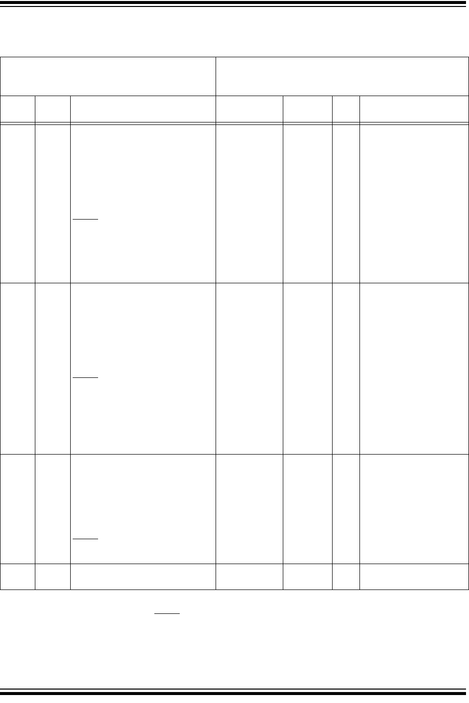
28.3 DC Characteristics: PIC18F2480/2580/4480/4580 (Industrial)
PIC18LF2480/2580/4480/4580 (Industrial)
DC CHARACTERISTICS
Standard Operating Conditions (unless otherwise stated)
Operating temperature -40°C ≤ TA ≤ +85°C for industrial
-40°C ≤ T
A ≤ +125°C for extended
Param
No.
Symbol Characteristic Min Max Units Conditions
V
IL Input Low Voltage
I/O Ports:
D030 with TTL Buffer V
SS 0.15 VDD VVDD < 4.5V
D030A — 0.8 V 4.5V ≤ VDD ≤ 5.5V
D031 with Schmitt Trigger Buffer VSS 0.2 VDD V
D031A
RC3 and RC4
VSS 0.3 Vdd V I
2
C™ enabled
D031B VSS 0.8 V SMBus enabled
D032 MCLR
VSS 0.2 VDD V
D033 OSC1 V
SS 0.3 VDD VHS, HSPLL modes
D033A OSC1 VSS 0.2 VDD V RC, EC modes
(1)
D033B OSC1 VSS 0.3 V XT, LP modes
D034 T13CKI V
SS 0.3 V
VIH Input High Voltage
I/O Ports:
D040 with TTL Buffer 0.25 V
DD + 0.8V VDD VVDD < 4.5V
D040A 2.0 VDD V4.5V ≤ VDD ≤ 5.5V
D041 with Schmitt Trigger Buffer 0.8 VDD VDD V
D041A
RC3 and RC4 0.7 V
DD
VDD V
I
2
C™ enabled
D041B 2.1 V
DD V SMBus enabled, VDD ≥ 3V
D042 MCLR
0.8 VDD VDD V
D043 OSC1 0.7 V
DD VDD VHS, HSPLL modes
D043A OSC1 0.8 VDD VDD VEC mode
D043B OSC1 0.9 VDD VDD V RC mode
(1)
D043C OSC1 1.6 VDD V XT, LP modes
D044 T13CKI 1.6 VDD V
I
IL Input Leakage Current
(2,3)
D060 I/O Ports — ±200 nA V
DD < 5.5V,
V
SS ≤ VPIN ≤ VDD,
Pin at high-impedance
— ±50 nA V
DD < 3V,
V
SS ≤ VPIN ≤ VDD,
Pin at high-impedance
D061 MCLR
— ±1 μAVss ≤ VPIN ≤ VDD
D063 OSC1 — ±1 μAVss ≤ VPIN ≤ VDD
I
PU Weak Pull-up Current
D070 I
PURB PORTB Weak Pull-up Current 50 400 μAVDD = 5V, VPIN = VSS
Note 1: In RC oscillator configuration, the OSC1/CLKI pin is a Schmitt Trigger input. It is not recommended that the
PIC
®
device be driven with an external clock while in RC mode.
2: The leakage current on the MCLR
pin is strongly dependent on the applied voltage level. The specified
levels represent normal operating conditions. Higher leakage current may be measured at different input
voltages.
3: Negative current is defined as current sourced by the pin.