
Datasheet


Table Of Contents
- Power-Managed Modes:
- Flexible Oscillator Structure:
- Special Microcontroller Features:
- Peripheral Highlights:
- ECAN Technology Module Features:
- Pin Diagrams
- Pin Diagrams (Continued)
- Table of Contents
- Most Current Data Sheet
- Errata
- Customer Notification System
- 1.0 Device Overview
- 2.0 Guidelines for Getting Started with PIC18F Microcontrollers
- 3.0 Oscillator Configurations
- 4.0 Power-Managed Modes
- 5.0 Reset
- 5.1 RCON Register
- 5.2 Master Clear Reset (MCLR)
- 5.3 Power-on Reset (POR)
- 5.4 Brown-out Reset (BOR)
- 5.5 Device Reset Timers
- 5.5.1 Power-up Timer (PWRT)
- 5.5.2 Oscillator Start-up Timer (OST)
- 5.5.3 PLL Lock Time-out
- 5.5.4 Time-out Sequence
- TABLE 5-2: Time-out in Various Situations
- FIGURE 5-3: Time-out Sequence on Power-up (MCLR Tied to Vdd, Vdd Rise < Tpwrt)
- FIGURE 5-4: Time-out Sequence on Power-up (MCLR Not Tied to Vdd): Case 1
- FIGURE 5-5: Time-out Sequence on Power-up (MCLR Not Tied to Vdd): Case 2
- FIGURE 5-6: Slow Rise Time (MCLR Tied to Vdd, Vdd Rise > Tpwrt)
- FIGURE 5-7: Time-out Sequence on POR w/PLL Enabled (MCLR Tied to Vdd)
- 5.6 Reset State of Registers
- 6.0 Memory Organization
- 6.1 Program Memory Organization
- 6.2 PIC18 Instruction Cycle
- 6.3 Data Memory Organization
- 6.4 Data Addressing Modes
- 6.5 Program Memory and the Extended Instruction Set
- 6.6 Data Memory and the Extended Instruction Set
- 7.0 Flash Program Memory
- 7.1 Table Reads and Table Writes
- 7.2 Control Registers
- 7.3 Reading the Flash Program Memory
- 7.4 Erasing Flash Program Memory
- 7.5 Writing to Flash Program Memory
- 7.6 Flash Program Operation During Code Protection
- 8.0 Data EEPROM Memory
- 9.0 8 x 8 Hardware Multiplier
- 9.1 Introduction
- 9.2 Operation
- EXAMPLE 9-1: 8 x 8 Unsigned Multiply Routine
- EXAMPLE 9-2: 8 x 8 Signed Multiply Routine
- TABLE 9-1: Performance Comparison for Various Multiply Operations
- EQUATION 9-1: 16 x 16 Unsigned Multiplication Algorithm
- EXAMPLE 9-3: 16 x 16 Unsigned Multiply Routine
- EQUATION 9-2: 16 x 16 Signed Multiplication Algorithm
- EXAMPLE 9-4: 16 x 16 Signed Multiply Routine
- 10.0 Interrupts
- 11.0 I/O Ports
- 12.0 Timer0 Module
- 13.0 Timer1 Module
- 14.0 Timer2 Module
- 15.0 Timer3 Module
- 16.0 Capture/Compare/PWM (CCP) Modules
- Register 16-1: CCP1CON: Capture/Compare/PWM Control Register
- 16.1 CCP Module Configuration
- 16.2 Capture Mode
- 16.3 Compare Mode
- 16.4 PWM Mode
- 17.0 Enhanced Capture/Compare/PWM (ECCP) Module
- Register 17-1: ECCP1CON Register (ECCP1 module, PIC18F4480/4580 Devices)
- 17.1 ECCP Outputs and Configuration
- 17.2 Capture and Compare Modes
- 17.3 Standard PWM Mode
- 17.4 Enhanced PWM Mode
- 18.0 Master Synchronous Serial Port (MSSP) Module
- 18.1 Master SSP (MSSP) Module Overview
- 18.2 Control Registers
- 18.3 SPI Mode
- 18.4 I2C Mode
- FIGURE 18-7: MSSP Block Diagram (I2C™ Mode)
- 18.4.1 Registers
- 18.4.2 Operation
- 18.4.3 Slave Mode
- 18.4.4 Clock Stretching
- 18.4.5 General Call Address Support
- 18.4.6 Master Mode
- 18.4.7 Baud Rate
- 18.4.8 I2C Master Mode Start Condition Timing
- 18.4.9 I2C Master Mode Repeated Start Condition Timing
- 18.4.10 I2C Master Mode Transmission
- 18.4.11 I2C Master Mode Reception
- 18.4.12 Acknowledge Sequence Timing
- 18.4.13 Stop Condition Timing
- 18.4.14 Sleep Operation
- 18.4.15 Effect of a Reset
- 18.4.16 Multi-Master Mode
- 18.4.17 Multi-Master Communication, Bus Collision and Bus Arbitration
- FIGURE 18-25: Bus Collision Timing for Transmit and Acknowledge
- FIGURE 18-26: Bus Collision During Start Condition (SDA Only)
- FIGURE 18-27: Bus Collision During Start Condition (SCL = 0)
- FIGURE 18-28: BRG Reset Due to SDA Arbitration During Start Condition
- FIGURE 18-29: Bus Collision During a Repeated Start Condition (Case 1)
- FIGURE 18-30: Bus Collision During Repeated Start Condition (Case 2)
- FIGURE 18-31: Bus Collision During a Stop Condition (Case 1)
- FIGURE 18-32: Bus Collision During a Stop Condition (Case 2)
- 19.0 Enhanced Universal Synchronous Receiver Transmitter (EUSART)
- Register 19-1: TXSTA: Transmit Status And Control Register
- Register 19-2: RCSTA: Receive Status And Control Register
- Register 19-3: BAUDCON: Baud Rate Control Register
- 19.1 Baud Rate Generator (BRG)
- 19.2 EUSART Asynchronous Mode
- 19.3 EUSART Synchronous Master Mode
- 19.4 EUSART Synchronous Slave Mode
- 20.0 10-Bit Analog-to-Digital Converter (A/D) Module
- Register 20-1: ADCON0: A/D Control Register 0
- Register 20-2: ADCON1: A/D Control Register 1
- Register 20-3: ADCON2: A/D Control Register 2
- FIGURE 20-1: A/D Block Diagram
- FIGURE 20-2: Analog Input Model
- 20.1 A/D Acquisition Requirements
- 20.2 Selecting and Configuring Automatic Acquisition Time
- 20.3 Selecting the A/D Conversion Clock
- 20.4 Operation in Power-Managed Modes
- 20.5 Configuring Analog Port Pins
- 20.6 A/D Conversions
- 20.7 Use of the CCP1 Trigger
- 21.0 Comparator Module
- Register 21-1: CMCON: Comparator Control Register
- 21.1 Comparator Configuration
- 21.2 Comparator Operation
- 21.3 Comparator Reference
- 21.4 Comparator Response Time
- 21.5 Comparator Outputs
- 21.6 Comparator Interrupts
- 21.7 Comparator Operation During Sleep
- 21.8 Effects of a Reset
- 21.9 Analog Input Connection Considerations
- 22.0 Comparator Voltage Reference Module
- 23.0 High/Low-Voltage Detect (HLVD)
- 24.0 ECAN Module
- 24.1 Module Overview
- 24.2 CAN Module Registers
- 24.2.1 CAN Control and Status Registers
- Register 24-1: CANCON: CAN Control Register
- Register 24-2: CANSTAT: CAN Status Register
- EXAMPLE 24-1: Changing to Configuration Mode
- EXAMPLE 24-2: WIN and ICODE Bits Usage in Interrupt Service Routine to Access TX/RX Buffers
- EXAMPLE 24-2: WIN and ICODE Bits Usage in Interrupt Service Routine to Access TX/RX Buffers (Continued)
- Register 24-3: ECANCON: Enhanced CAN Control Register
- Register 24-4: COMSTAT: Communication Status Register
- 24.2.2 Dedicated CAN Transmit Buffer Registers
- Register 24-5: TXBnCON: Transmit Buffer n Control Registers [0 £ n £ 2]
- Register 24-6: TXBnSIDH: Transmit Buffer n Standard Identifier Registers, High Byte [0 £ n £ 2]
- Register 24-7: TXBnSIDL: Transmit Buffer n Standard Identifier Registers, Low Byte [0 £ n £ 2]
- Register 24-8: TXBnEIDH: Transmit Buffer n Extended Identifier Registers, High Byte [0 £ n £ 2]
- Register 24-9: TXBnEIDL: Transmit Buffer n Extended Identifier Registers, Low Byte [0 £ n £ 2]
- Register 24-10: TXBnDm: Transmit Buffer n Data Field Byte m Registers [0 £ n £ 2, 0 £ m £ 7]
- Register 24-11: TXBnDLC: Transmit Buffer n Data Length Code Registers [0 £ n £ 2]
- Register 24-12: TXERRCNT: Transmit Error Count Register
- EXAMPLE 24-3: Transmitting a CAN Message Using Banked Method
- EXAMPLE 24-4: Transmitting a CAN Message Using WIN Bits
- 24.2.3 Dedicated CAN Receive Buffer Registers
- Register 24-13: RXB0CON: Receive Buffer 0 Control Register
- Register 24-14: RXB1CON: Receive Buffer 1 Control Register
- Register 24-15: RXBnSIDH: Receive Buffer n Standard Identifier Registers, High Byte [0 £ n £ 1]
- Register 24-16: RXBnSIDL: Receive Buffer n Standard Identifier Registers, Low Byte [0 £ n £ 1]
- Register 24-17: RXBnEIDH: Receive Buffer n Extended Identifier Registers, High Byte [0 £ n £ 1]
- Register 24-18: RXBnEIDL: Receive Buffer n Extended Identifier Registers, Low Byte [0 £ n £ 1]
- Register 24-19: RXBnDLC: Receive Buffer n Data Length Code Registers [0 £ n £ 1]
- Register 24-20: RXBnDm: Receive Buffer n Data Field Byte m Registers [0 £ n £ 1, 0 £ m £ 7]
- Register 24-21: RXERRCNT: Receive Error Count Register
- EXAMPLE 24-5: Reading a CAN Message
- Register 24-22: BnCON: TX/RX Buffer n Control Registers in Receive Mode [0 £ n £ 5, TXnEN (bsel0
) = 0](1) - Register 24-23: BnCON: TX/RX Buffer n Control Registers in Transmit Mode [0 £ n £ 5, TXnEN (bsel0
) = 1](1) - Register 24-24: BnSIDH: TX/RX Buffer n Standard Identifier Registers, High Byte in Receive Mode [0 £ n £ 5, TXnEN (BSEL0
) = 0](1) - Register 24-25: BnSIDH: TX/RX Buffer n Standard Identifier Registers, High Byte in Transmit Mode [0 £ n £ 5, TXnEN (BSEL0
) = 1](1) - Register 24-26: BnSIDL: TX/RX Buffer n Standard Identifier Registers, Low Byte in Receive Mode [0 £ n £ 5, TXnEN (bsel0
) = 0](1) - Register 24-27: BnSIDL: TX/RX Buffer n Standard Identifier Registers, Low Byte in Receive Mode [0 £ n £ 5, TXnEN (bsel0
) = 1](1) - Register 24-28: BnEIDH: TX/RX Buffer n Extended Identifier Registers, High Byte in Receive Mode [0 £ n £ 5, TXnEN (BSEL0
) = 0](1) - Register 24-29: BnEIDH: TX/RX Buffer n Extended Identifier Registers, High Byte in Transmit Mode [0 £ n £ 5, TXnEN (BSEL0
) = 1](1) - Register 24-30: BnEIDL: TX/RX Buffer n Extended Identifier Registers, Low Byte in Receive Mode [0 £ n £ 5, TXnEN (BSEL
) = 0](1) - Register 24-31: BnEIDL: TX/RX Buffer n Extended Identifier Registers, Low Byte in Receive Mode [0 £ n £ 5, TXnEN (BSEL
) = 1](1) - Register 24-32: BnDm: TX/RX Buffer n Data Field Byte m Registers in Receive Mode [0 £ n £ 5, 0 £ m £ 7, TXnEN (BSEL
) = 0](1) - Register 24-33: BnDm: TX/RX Buffer n Data Field Byte m Registers in Transmit Mode [0 £ n £ 5, 0 £ m £ 7, TXnEN (BSEL
) = 1](1) - Register 24-34: BnDLC: TX/RX Buffer n Data Length Code Registers in Receive Mode [0 £ n £ 5, TXnEN (BSEL
) = 0](1) - Register 24-35: BnDLC: TX/RX Buffer n Data Length Code Registers in Transmit Mode [0 £ n £ 5, TXnEN (BSEL
) = 1](1) - Register 24-36: BSEL0: Buffer Select Register 0(1)
- Register 24-37: RXFnSIDH: Receive Acceptance Filter n Standard Identifier Filter Registers, High Byte [0 £ n £ 15](1)
- Register 24-38: RXFnSIDL: Receive Acceptance Filter n Standard Identifier Filter Registers, Low Byte [0 £ n £ 15](1)
- Register 24-39: RXFnEIDH: Receive Acceptance Filter n Extended Identifier Registers, High Byte [0 £ n £ 15](1)
- Register 24-40: RXFnEIDL: Receive Acceptance Filter n Extended Identifier Registers, Low Byte [0 £ n £ 15](1)
- Register 24-41: RXMnSIDH: Receive Acceptance Mask n Standard Identifier Mask Registers, High Byte [0 £ n £ 1]
- Register 24-42: RXMnSIDL: Receive Acceptance Mask n Standard Identifier Mask Registers, Low Byte [0 £ n £ 1]
- Register 24-43: RXMnEIDH: Receive Acceptance Mask n Extended Identifier Mask Registers, High Byte [0 £ n £ 1]
- Register 24-44: RXMnEIDL: Receive Acceptance Mask n Extended Identifier Mask Registers, Low Byte [0 £ n £ 1]
- Register 24-45: RXFCONn: Receive Filter Control Register n [0 £ n £ 1](1)
- Register 24-46: SDFLC: Standard Data Bytes Filter Length Count Register(1)
- Register 24-47: RXFBCONn: Receive Filter Buffer Control Register n(1)
- Register 24-48: MSEL0: Mask Select Register 0(1)
- Register 24-49: MSEL1: Mask Select Register 1(1)
- Register 24-50: MSEL2: Mask Select Register 2(1)
- Register 24-51: MSEL3: Mask Select Register 3(1)
- 24.2.4 CAN Baud Rate Registers
- 24.2.5 CAN Module I/O Control Register
- 24.2.6 CAN Interrupt Registers
- Register 24-56: PIR3: Peripheral Interrupt Request (Flag) Register 3
- Register 24-57: PIE3: Peripheral Interrupt Enable Register 3
- Register 24-58: IPR3: Peripheral Interrupt Priority Register 3
- Register 24-59: TXBIE: Transmit Buffers Interrupt Enable Register(1)
- Register 24-60: BIE0: Buffer Interrupt Enable Register 0(1)
- TABLE 24-1: Can Controller Register Map
- TABLE 24-1: Can Controller Register Map (continued)
- 24.2.1 CAN Control and Status Registers
- 24.3 CAN Modes of Operation
- 24.4 CAN Module Functional Modes
- 24.5 CAN Message Buffers
- 24.6 CAN Message Transmission
- 24.7 Message Reception
- 24.8 Message Acceptance Filters and Masks
- 24.9 Baud Rate Setting
- EQUATION 24-1:
- EQUATION 24-2:
- EQUATION 24-3:
- FIGURE 24-4: Bit Time Partitioning
- 24.9.1 External Clock, Internal Clock and Measurable Jitter in HS-PLL Based Oscillators
- 24.9.2 Time Quanta
- 24.9.3 Synchronization Segment
- 24.9.4 Propagation Segment
- 24.9.5 Phase Buffer Segments
- 24.9.6 Sample Point
- 24.9.7 Information Processing Time
- 24.10 Synchronization
- 24.11 Programming Time Segments
- 24.12 Oscillator Tolerance
- 24.13 Bit Timing Configuration Registers
- 24.14 Error Detection
- 24.15 CAN Interrupts
- 25.0 Special Features of the CPU
- 25.1 Configuration Bits
- TABLE 25-1: Configuration Bits and Device IDs
- Register 25-1: CONFIG1H: Configuration Register 1 High (Byte Address 300001h)
- Register 25-2: CONFIG2L: Configuration Register 2 Low (Byte Address 300002h)
- Register 25-3: CONFIG2H: Configuration Register 2 High (Byte Address 300003h)
- Register 25-4: CONFIG3H: Configuration Register 3 High (Byte Address 300005h)
- Register 25-5: CONFIG4L: Configuration Register 4 Low (Byte Address 300006h)
- Register 25-6: CONFIG5L: Configuration Register 5 Low (Byte Address 300008h)
- Register 25-7: CONFIG5H: Configuration Register 5 High (Byte Address 300009h)
- Register 25-8: CONFIG6L: Configuration Register 6 Low (Byte Address 30000Ah)
- Register 25-9: CONFIG6H: Configuration Register 6 High (Byte Address 30000Bh)
- Register 25-10: CONFIG7L: Configuration Register 7 Low (Byte Address 30000Ch)
- Register 25-11: CONFIG7H: Configuration Register 7 High (Byte Address 30000Dh)
- Register 25-12: DEVID1: Device ID Register 1 for PIC18F2480/2580/4480/4580
- Register 25-13: DEVID2: Device ID Register 2 for PIC18F2480/2580/4480/4580
- 25.2 Watchdog Timer (WDT)
- 25.3 Two-Speed Start-up
- 25.4 Fail-Safe Clock Monitor
- 25.5 Program Verification and Code Protection
- 25.6 ID Locations
- 25.7 In-Circuit Serial Programming
- 25.8 In-Circuit Debugger
- 25.9 Single-Supply ICSP Programming
- 25.1 Configuration Bits
- 26.0 Instruction Set Summary
- 26.1 Standard Instruction Set
- 26.2 Extended Instruction Set
- 27.0 Development Support
- 27.1 MPLAB Integrated Development Environment Software
- 27.2 MPLAB C Compilers for Various Device Families
- 27.3 HI-TECH C for Various Device Families
- 27.4 MPASM Assembler
- 27.5 MPLINK Object Linker/ MPLIB Object Librarian
- 27.6 MPLAB Assembler, Linker and Librarian for Various Device Families
- 27.7 MPLAB SIM Software Simulator
- 27.8 MPLAB REAL ICE In-Circuit Emulator System
- 27.9 MPLAB ICD 3 In-Circuit Debugger System
- 27.10 PICkit 3 In-Circuit Debugger/ Programmer and PICkit 3 Debug Express
- 27.11 PICkit 2 Development Programmer/Debugger and PICkit 2 Debug Express
- 27.12 MPLAB PM3 Device Programmer
- 27.13 Demonstration/Development Boards, Evaluation Kits, and Starter Kits
- 28.0 Electrical Characteristics
- Absolute Maximum Ratings (†)
- 28.1 DC Characteristics: Supply Voltage PIC18F2480/2580/4480/4580 (Industrial, Extended) PIC18LF2480/2580/4480/4580 (Industrial)
- 28.2 DC Characteristics: Power-Down and Supply Current PIC18F2480/2580/4480/4580 (Industrial, Extended) PIC18LF2480/2580/4480/4580 (Industrial)
- 28.3 DC Characteristics: PIC18F2480/2580/4480/4580 (Industrial) PIC18LF2480/2580/4480/4580 (Industrial)
- 28.4 AC (Timing) Characteristics
- 28.4.1 Timing Parameter Symbology
- 28.4.2 Timing Conditions
- 28.4.3 Timing Diagrams and Specifications
- FIGURE 28-5: External Clock Timing (All Modes Except PLL)
- TABLE 28-6: External Clock Timing Requirements
- TABLE 28-7: PLL Clock Timing Specifications (Vdd = 4.2V to 5.5V)
- TABLE 28-8: AC Characteristics: Internal RC Accuracy PIC18F2480/2580/4480/4580 (Industrial) PIC18LF2480/2580/4480/4580 (Industrial)
- FIGURE 28-6: CLKO and I/O Timing
- TABLE 28-9: CLKO and I/O Timing Requirements
- FIGURE 28-7: Reset, Watchdog Timer, Oscillator Start-up Timer and Power-up Timer Timing
- FIGURE 28-8: Brown-out Reset Timing
- TABLE 28-10: Reset, Watchdog Timer, Oscillator Start-up Timer, Power-up Timer and Brown-out Reset Requirements
- FIGURE 28-9: Timer0 and Timer1 External Clock Timings
- TABLE 28-11: Timer0 and Timer1 External Clock Requirements
- FIGURE 28-10: Capture/Compare/PWM Timings (All CCP Modules)
- TABLE 28-12: Capture/Compare/PWM Requirements (All CCP Modules)
- FIGURE 28-11: Parallel Slave Port Timing (PIC18F4480/4580)
- TABLE 28-13: Parallel Slave Port Requirements (PIC18F4480/4580)
- FIGURE 28-12: Example SPI Master Mode Timing (CKE = 0)
- TABLE 28-14: Example SPI Mode Requirements (Master Mode, CKE = 0)
- FIGURE 28-13: Example SPI Master Mode Timing (CKE = 1)
- TABLE 28-15: Example SPI Mode Requirements (Master Mode, CKE = 1)
- FIGURE 28-14: Example SPI Slave Mode Timing (CKE = 0)
- TABLE 28-16: Example SPI Mode Requirements (Slave Mode Timing, CKE = 0)
- FIGURE 28-15: Example SPI Slave Mode Timing (CKE = 1)
- TABLE 28-17: Example SPI Slave Mode Requirements (CKE = 1)
- FIGURE 28-16: I2C™ Bus Start/Stop Bits Timing
- TABLE 28-18: I2C™ Bus Start/Stop Bits Requirements (Slave Mode)
- FIGURE 28-17: I2C™ Bus Data Timing
- TABLE 28-19: I2C™ Bus Data Requirements (Slave Mode)
- FIGURE 28-18: Master SSP I2C™ Bus Start/Stop Bits Timing Waveforms
- TABLE 28-20: Master SSP I2C™ Bus Start/Stop Bits Requirements
- FIGURE 28-19: Master SSP I2C™ Bus Data Timing
- TABLE 28-21: Master SSP I2c™ Bus Data Requirements
- FIGURE 28-20: EUSART Synchronous Transmission (Master/Slave) Timing
- TABLE 28-22: EUSART Synchronous Transmission Requirements
- FIGURE 28-21: EUSART Synchronous Receive (Master/Slave) Timing
- TABLE 28-23: EUSART Synchronous Receive Requirements
- TABLE 28-24: A/D Converter Characteristics: PIC18F2480/2580/4480/4580 (Industrial) PIC18LF2480/2580/4480/4580 (Industrial)
- FIGURE 28-22: A/D Conversion Timing
- TABLE 28-25: A/D Conversion Requirements
- 29.0 Packaging Information
- Appendix A: Revision History
- Appendix B: Device Differences
- Appendix C: Conversion Considerations
- Appendix D: Migration from Baseline to Enhanced Devices
- Appendix E: Migration From Mid-Range to Enhanced Devices
- Appendix F: Migration From High-End to Enhanced Devices
- INDEX
- The Microchip Web Site
- Customer Change Notification Service
- Customer Support
- Reader Response
- PIC18F2480/2580/4480/4580 Product Identification System
- Worldwide Sales and Service
PIC18F2480/2580/4480/4580
DS39637D-page 346 © 2009 Microchip Technology Inc.
24.15.1 INTERRUPT CODE BITS
To simplify the interrupt handling process in user firm-
ware, the ECAN module encodes a special set of bits. In
Mode 0, these bits are ICODE<3:1> in the CANSTAT
register. In Mode 1 and 2, these bits are EICODE<4:0> in
the CANSTAT register. Interrupts are internally prioritized
such that the higher priority interrupts are assigned lower
values. Once the highest priority interrupt condition has
been cleared, the code for the next highest priority inter-
rupt that is pending (if any) will be reflected by the ICODE
bits (see Table 24-5). Note that only those interrupt
sources that have their associated interrupt enable bit set
will be reflected in the ICODE bits.
In Mode 2, when a receive message interrupt occurs,
the EICODE bits will always consist of ‘10000’. User
firmware may use FIFO Pointer bits to actually access
the next available buffer.
24.15.2 TRANSMIT INTERRUPT
When the transmit interrupt is enabled, an interrupt will
be generated when the associated transmit buffer
becomes empty and is ready to be loaded with a new
message. In Mode 0, there are separate interrupt enable/
disable and flag bits for each of the three dedicated trans-
mit buffers. The TXBnIF bit will be set to indicate the
source of the interrupt. The interrupt is cleared by the
MCU, resetting the TXBnIF bit to a ‘0’. In Mode 1 and 2,
all transmit buffers share one interrupt enable/disable bit
and one flag bit. In Mode 1 and 2, TXBIE in PIE3 and
TXBIF in PIR3 indicate when a transmit buffer has com-
pleted transmission of its message. TXBnIF, TXBnIE and
TXBnIP in PIR3, PIE3 and IPR3, respectively, are not
used in Mode 1 and 2. Individual transmit buffer interrupts
can be enabled or disabled by setting or clearing TXBIE
and B0IE register bits. When a shared interrupt occurs,
user firmware must poll the TXREQ bit of all transmit
buffers to detect the source of interrupt.
24.15.3 RECEIVE INTERRUPT
When the receive interrupt is enabled, an interrupt will
be generated when a message has been successfully
received and loaded into the associated receive buffer.
This interrupt is activated immediately after receiving
the End-Of-Frame (EOF) field.
In Mode 0, the RXBnIF bit is set to indicate the source
of the interrupt. The interrupt is cleared by the MCU,
resetting the RXBnIF bit to a ‘0’.
In Mode 1 and 2, all receive buffers share RXBIE,
RXBIF and RXBIP in PIE3, PIR3 and IPR3, respec-
tively. Bits, RXBnIE, RXBnIF and RXBnIP, are not
used. Individual receive buffer interrupts can be con-
trolled by the TXBIE and BIE0 registers. In Mode 1,
when a shared receive interrupt occurs, user firmware
must poll the RXFUL bit of each receive buffer to detect
the source of interrupt. In Mode 2, a receive interrupt
indicates that the new message is loaded into FIFO.
FIFO can be read by using FIFO Pointer bits, FP.
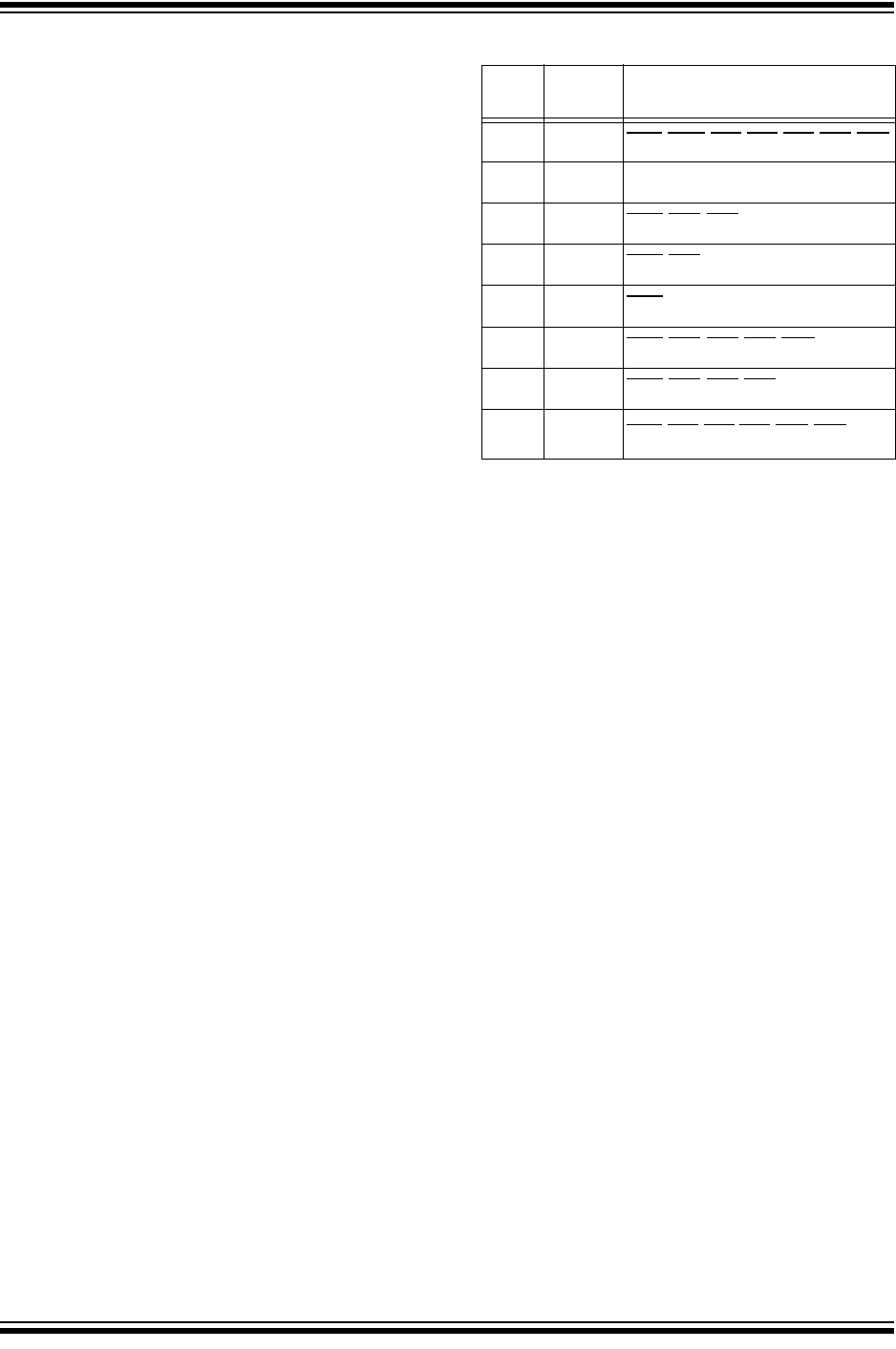
TABLE 24-5: VALUES FOR ICODE<2:0>
24.15.4 MESSAGE ERROR INTERRUPT
When an error occurs during transmission or reception
of a message, the message error flag, IRXIF, will be set
and if the IRXIE bit is set, an interrupt will be generated.
This is intended to be used to facilitate baud rate
determination when used in conjunction with Listen
Only mode.
24.15.5 BUS ACTIVITY WAKE-UP
INTERRUPT
When the PIC18F2480/2580/4480/4580 devices are in
Sleep mode and the bus activity wake-up interrupt is
enabled, an interrupt will be generated and the WAKIF
bit will be set when activity is detected on the CAN bus.
This interrupt causes the PIC18F2480/2580/4480/
4580 devices to exit Sleep mode. The interrupt is reset
by the MCU, clearing the WAKIF bit.
24.15.6 ERROR INTERRUPT
When the CAN module error interrupt (ERRIE in PIE3)
is enabled, an interrupt is generated if an overflow con-
dition occurs, or if the error state of the transmitter or
receiver has changed. The error flags in COMSTAT will
indicate one of the following conditions.
ICODE
<2:0>
Interrupt Boolean Expression
000 None ERR
•WAK•TX0•TX1•TX2•RX0•RX1
001 Error ERR
010 TXB2 ERR•TX0•TX1•TX2
011 TXB1 ERR•TX0•TX1
100 TXB0 ERR•TX0
101 RXB1 ERR•TX0•TX1•TX2•RX0•RX1
110 RXB0 ERR•TX0•TX1•TX2•RX0
111
Wake on
Interrupt
ERR
•TX0•TX1•TX2•RX0•RX1•WAK
Legend:
ERR = ERRIF * ERRIE RX0 = RXB0IF * RXB0IE
TX0 = TXB0IF * TXB0IE RX1 = RXB1IF * RXB1IE
TX1 = TXB1IF * TXB1IE WAK = WAKIF * WAKIE
TX2 = TXB2IF * TXB2IE