
Datasheet


PIC18F2455/2550/4455/4550
DS39632E-page 404 © 2009 Microchip Technology Inc.
TABLE 28-28: A/D CONVERTER CHARACTERISTICS: PIC18F2455/2550/4455/4550 (INDUSTRIAL)
PIC18LF2455/2550/4455/4550 (INDUSTRIAL)
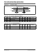
FIGURE 28-23: A/D CONVERSION TIMING
Param
No.
Symbol Characteristic Min Typ Max Units Conditions
A01 N
R Resolution — — 10 bit ΔVREF ≥ 3.0V
A03 EIL Integral Linearity Error — — <±1 LSB ΔVREF ≥ 3.0V
A04 E
DL Differential Linearity Error — — <±1 LSB ΔVREF ≥ 3.0V
A06 EOFF Offset Error — — <±2.0 LSB ΔVREF ≥ 3.0V
A07 EGN Gain Error — — <±1 LSB ΔVREF ≥ 3.0V
A10 — Monotonicity Guaranteed
(1)
—VSS ≤ VAIN ≤ VREF
A20 ΔVREF Reference Voltage Range
(V
REFH – VREFL)
1.8
3.0
—
—
V
DD – VSS
V
DD – VSS
V
V
V
DD < 3.0V
V
DD ≥ 3.0V
A21 V
REFH Reference Voltage High Vss +
ΔV
REF
—VDD V
A22 V
REFL Reference Voltage Low VSS —VDD - ΔVREF V
A25 V
AIN Analog Input Voltage VREFL —VREFH V
A30 ZAIN Recommended Impedance of
Analog Voltage Source
——2.5kΩ
A50 I
REF VREF Input Current
(2)
—
—
—
—
5
150
μA
μA
During VAIN acquisition.
During A/D conversion
cycle.
Note 1: The A/D conversion result never decreases with an increase in the input voltage and has no missing codes.
2: V
REFH current is from RA3/AN3/VREF+ pin or VDD, whichever is selected as the VREFH source.
V
REFL current is from RA2/AN2/VREF-/CVREF pin or VSS, whichever is selected as the VREFL source.
131
130
132
BSF ADCON0, GO
Q4
A/D CLK
A/D DATA
ADRES
ADIF
GO
SAMPLE
OLD_DATA
SAMPLING STOPPED
DONE
NEW_DATA
(Note 2)
987 321
Note 1: If the A/D clock source is selected as RC, a time of T
CY is added before the A/D clock starts.
This allows the SLEEP instruction to be executed.
2: This is a minimal RC delay (typically 100 ns), which also disconnects the holding capacitor from the analog input.
. . .
. . .
TCY
(1)
0
TDIS