
Information
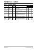
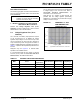
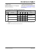
Table Of Contents
- TABLE 1: Silicon DEVREV Values
- TABLE 2: Silicon Issue Summary
- Silicon Errata Issues
- Data Sheet Clarifications
- Appendix A: Document Revision History
- Worldwide Sales and Service
2011 Microchip Technology Inc. DS80503E-page 3
PIC18F47J13 FAMILY
Silicon Errata Issues
1. Module: Charge Time Measurement Unit
(CTMU)
When using the CTMU, the constant current
source may not output if the internal band gap
reference is not enabled.
Work around
Before using the CTMU, the internal band gap ref-
erence module should be manually enabled by
setting the VBGEN bit to ‘1’ (ANCON1<7> = 1).
Affected Silicon Revisions
2. Module: Phase Locked Loop (PLL)
When OSCCON<6:4> are configured to settings
other than a 4 MHz or 8 MHz INTOSC post-
scaler, the PLLEN bit (OSCTUNE<6>) is forced
to ‘0’, even if firmware tries to set the PLLEN bit.
This may prevent firmware from enabling the
PLL.
Work around
Before attempting to set the PLLEN bit, config-
ure OSCCON<6:4> to ‘0b110’ or ‘0b111’ to
select the 4 MHz or 8 MHz INTOSC postscaler.
Affected Silicon Revisions
3. Module: Analog-to-Digital Converter
(ADC)
At the beginning of sample acquisition, one or
more small, pull-up pulses (approximately 25 ns
long) may output to the currently selected ANx
analog channel. These pulses can lead to a pos-
itive offset error when the analog signal voltage
is near V
SS and the external analog signal driver
is unable to dissipate the added pull-up voltage
before the A/D conversion occurs.
Work around
Do one or more of the following:
• Use the “0 T
AD” A/D acquisition time setting to
start the next sample acquisition period imme-
diately following an A/D conversion
completion.
This allows the external analog signal driver
more time to dissipate the pull-up pulses that
occur when the sample acquisition is started.
• Use a longer A/D acquisition time setting to
provide time for the external analog signal
driver to dissipate the pull-up pulse voltage.
• Use low-impedance, active analog signal
drivers to reduce the time needed to dissipate
the pull-up pulse voltage.
• Experiment with external filter capacitor val-
ues to avoid allowing the pull-up voltage offset
to affect the final voltage that gets converted.
Small filter capacitor values (or none at all) will
allow time for the external analog signal driver to
dissipate the pull-up voltage quickly. Alternately,
large filter capacitor values will prevent the short
pull-up pulses from increasing the final voltage,
enough to cause A/D conversion error.
Affected Silicon Revisions
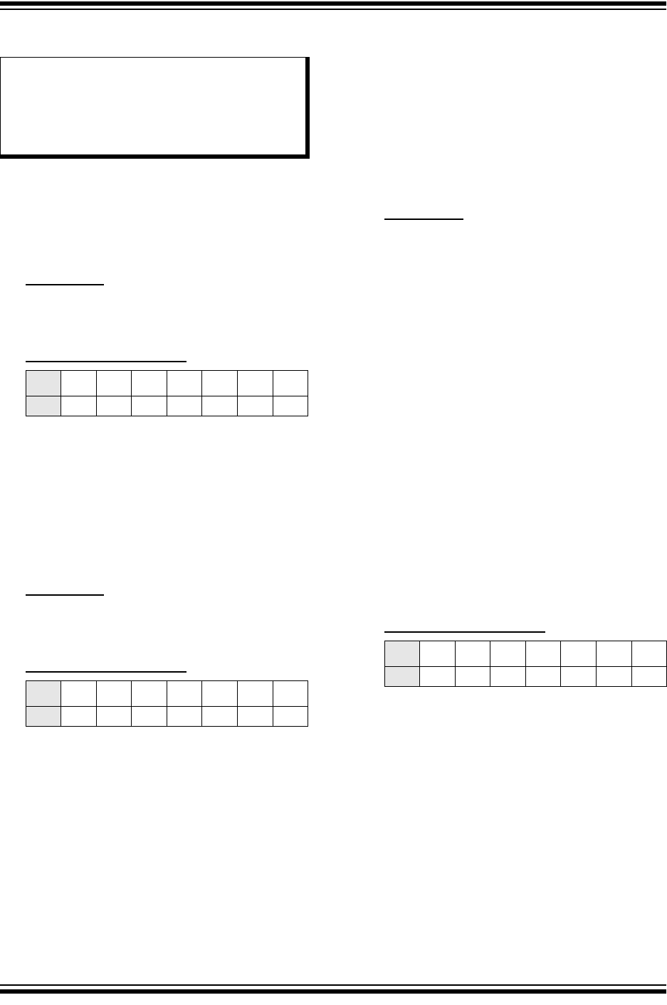
Note: This document summarizes all silicon
errata issues from all revisions of silicon,
previous as well as current. Only the
issues indicated by the shaded column in
the following tables apply to the current
silicon revision (A1).
A1
X
A1
X
A1
X