
Information
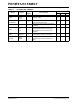
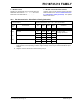
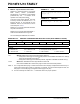
Table Of Contents
- TABLE 1: Silicon DEVREV Values
- TABLE 2: Silicon Issue Summary
- Silicon Errata Issues
- Data Sheet Clarifications
- Appendix A: Document Revision History
- Worldwide Sales and Service

PIC18F47J13 FAMILY
DS80503E-page 2 2011 Microchip Technology Inc.
TABLE 2: SILICON ISSUE SUMMARY
Module Feature
Item
Number
Issue Summary
Affected Revisions
(1)
A1
CTMU
Constant
Current
Source
1.
Band gap must be manually enabled before
using the CTMU. X
Oscillator
Configurations
PLL 2.
PLL can not be enabled unless the 8 or
4 MHz INTOSC option is set.
X
ADC A/D 3.
ANx pin may output a pull-up pulse during
acquisition.
X
MSSP
I
2
C™
Mode
4.
If a Stop condition occurs in the middle of an
address or data reception, there will be
issues with the SCL clock stream and
RCEN bit.
X
MSSP
I
2
C Slave
Reception
5.
In I
2
C slave reception, the module may
have problems receiving correct data.
X
EUSART
Enable/
Disable
6.
If interrupts are enabled, disabling and
re-enabling the module requires a 2 TCY
delay.
X
Note 1: Only those issues indicated in the last column apply to the current silicon revision.