
Datasheet


PIC18F2XK20/4XK20
DS41303G-page 76 2010 Microchip Technology Inc.
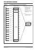
FIGURE 5-9: USE OF THE BANK SELECT REGISTER (DIRECT ADDRESSING)
Note 1: The Access RAM bit of the instruction can be used to force an override of the selected bank (BSR<3:0>) to
the registers of the Access Bank.
2: The MOVFF instruction embeds the entire 12-bit address in the instruction.
Data
Memory
Bank Select
(2)
7
0
From Opcode
(2)
0000
000h
100h
200h
300h
F00h
E00h
FFFh
Bank 0
Bank 1
Bank 2
Bank 14
Bank 15
00h
FFh
00h
FFh
00h
FFh
00h
FFh
00h
FFh
00h
FFh
Bank 3
through
Bank 13
0011
11111111
7
0
BSR
(1)