
Datasheet


PIC18F2XK20/4XK20
DS41303G-page 286 2010 Microchip Technology Inc.
20.7 Analog Input Connection
Considerations
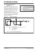
A simplified circuit for an analog input is shown in
Figure 20-6. Since the analog input pins share their
connection with a digital input, they have reverse
biased ESD protection diodes to V
DD and VSS. The
analog input, therefore, must be between V
SS and VDD.
If the input voltage deviates from this range by more
than 0.6V in either direction, one of the diodes is
forward biased and a latch-up may occur.
A maximum source impedance of 10 k is recommended
for the analog sources. Also, any external component
connected to an analog input pin, such as a capacitor or
a Zener diode, should have very little leakage current to
minimize inaccuracies introduced.
FIGURE 20-6: ANALOG INPUT MODEL
Note 1: When reading a PORT register, all pins
configured as analog inputs will read as a
‘0’. Pins configured as digital inputs will
convert as an analog input, according to
the input specification.
2: Analog levels on any pin defined as a
digital input, may cause the input buffer to
consume more current than is specified.
VA
Rs < 10K
C
PIN
5 pF
V
DD
RIC
ILEAKAGE
(1)
Vss
AIN
Legend: CPIN = Input Capacitance
I
LEAKAGE = Leakage Current at the pin due to various junctions
R
IC = Interconnect Resistance
R
S = Source Impedance
V
A = Analog Voltage
Note 1: See Section 26.0 “Electrical Characteristics”.