
Information


2008-2013 Microchip Technology Inc. DS80000404H-page 5
PIC18F26K20/46K20
12. Module: ADC
After extended stress the Most Significant bit
(MSb) of the ADC conversion result can become
stuck at ‘0’. Conversions resulting in code 511 or
less are still accurate, but conversions that should
result in codes greater than 511 are instead pinned
at 511.
The potential for failures is a function of several
factors:
• The potential for failures increases over the life
of the part. No failures have ever been seen for
accelerated stress estimated to be equivalent
to 34 years at room temperature. The failure
rate after accelerated stress estimated to be
equivalent to 146 years at room temperature
can be as high as 10% for V
DD = 1.8V. The time
to failure will decrease as the operating
temperature increases.
• The potential for failures is highest at low V
DD
and decreases as V
DD increases.
Work around
1. Restrict the input voltage to less than 1/2 of the
ADC voltage reference so that the expected
result is always a code less than or equal to 511.
2. Use manual acquisition time (ACQT<2:0> =
000) and put the part to Sleep after each
conversion.
Affected Silicon Revisions
13. Module: Interrupt-on-Change
When any interrupt-on-change is enabled and the
corresponding input is high, then waking from
Sleep by a source other than interrupt-on-change
may cause the RBIF interrupt flag bit to become
set improperly.
Work around
1. Use the INTx interrupts in lieu of interrupt-on-
change.
Or
2. Store the state of the PORTB inputs before
entering Sleep. Upon waking, if an RBIF is
detected, then compare the PORTB levels with
those stored. If they are the same, then clear
and ignore the RBIF interrupt.
Affected Silicon Revisions
14. Module: Capture/Compare/PWM
14.1 CCP2
The weak pull-up (if enabled) on the selected
CCP2 pin will be disabled when CCP2 is set up for
Capture mode.
Work around
Use an external resistor as the pull-up.
Affected Silicon Revisions
15. Module: Low-Voltage Detect
If Low-Voltage Detect is enabled, the band gap is
disabled in Sleep, and the part is put to Sleep for a
short period of time, the LVD will trigger
immediately upon waking-up from Sleep.
Work around
Do not disable the band gap in Sleep when using
the LVD.
Affected Silicon Revisions
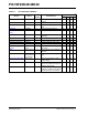
B2 B3 B5 B6
XX
B2 B3 B5 B6
XX
X X
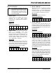
B2 B3 B5 B6
XX
X X
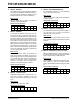
B2 B3 B5 B6
XX
X X