
Information


PIC18F2XK20/4XK20
DS41303G-page 80 2010 Microchip Technology Inc.
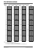
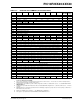
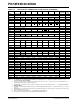
TMR0H Timer0 Register, High Byte 0000 0000 60, 157
TMR0L Timer0 Register, Low Byte xxxx xxxx 60, 157
T0CON TMR0ON T08BIT T0CS T0SE PSA T0PS2 T0PS1 T0PS0 1111 1111 60, 155
OSCCON IDLEN IRCF2 IRCF1 IRCF0 OSTS IOFS SCS1 SCS0 0011 qq00 29, 60
HLVDCON VDIRMAG
— IRVST HLVDEN HLVDL3 HLVDL2 HLVDL1 HLVDL0 0-00 0101 60, 293
WDTCON
— — — — — — —SWDTEN--- ---0 60, 309
RCON IPEN SBOREN
(1)
—RITO PD POR BOR 0q-1 11q0 51, 58,
118
TMR1H Timer1 Register, High Byte xxxx xxxx 60, 165
TMR1L Timer1 Register, Low Bytes xxxx xxxx 60, 165
T1CON RD16 T1RUN T1CKPS1 T1CKPS0 T1OSCEN T1SYNC
TMR1CS TMR1ON 0000 0000 60, 159
TMR2 Timer2 Register 0000 0000 60, 168
PR2 Timer2 Period Register 1111 1111 60, 168
T2CON
— T2OUTPS3 T2OUTPS2 T2OUTPS1 T2OUTPS0 TMR2ON T2CKPS1 T2CKPS0 -000 0000 60, 167
SSPBUF SSP Receive Buffer/Transmit Register xxxx xxxx 60, 201,
202
SSPADD SSP Address Register in I
2
C™ Slave Mode. SSP Baud Rate Reload Register in I
2
C Master Mode. 0000 0000 60, 202
SSPSTAT SMP CKE D/A
PSR/WUA BF 0000 0000 60, 194,
204
SSPCON1 WCOL SSPOV SSPEN CKP SSPM3 SSPM2 SSPM1 SSPM0 0000 0000 60, 195,
205
SSPCON2 GCEN ACKSTAT ACKDT ACKEN RCEN PEN RSEN SEN 0000 0000 60, 206
ADRESH A/D Result Register, High Byte xxxx xxxx 61, 277
ADRESL A/D Result Register, Low Byte xxxx xxxx 61, 277
ADCON0
— — CHS3 CHS2 CHS1 CHS0 GO/DONE ADON --00 0000 61, 271
ADCON1
— —VCFG1VCFG0— — — — --00 ---- 59, 272
ADCON2 ADFM
— ACQT2 ACQT1 ACQT0 ADCS2 ADCS1 ADCS0 0-00 0000 61, 273
CCPR1H Capture/Compare/PWM Register 1, High Byte xxxx xxxx 61, 144
CCPR1L Capture/Compare/PWM Register 1, Low Byte xxxx xxxx 61, 144
CCP1CON P1M1 P1M0 DC1B1 DC1B0 CCP1M3 CCP1M2 CCP1M1 CCP1M0 0000 0000 61, 173
CCPR2H Capture/Compare/PWM Register 2, High Byte xxxx xxxx 61, 144
CCPR2L Capture/Compare/PWM Register 2, Low Byte xxxx xxxx 61, 144
CCP2CON
— — DC2B1 DC2B0 CCP2M3 CCP2M2 CCP2M1 CCP2M0 --00 0000 61, 143
PSTRCON
— — — STRSYNC STRD STRC STRB STRA ---0 0001 61, 187
BAUDCON ABDOVF RCIDL DTRXP CKTXP BRG16
— WUE ABDEN 0100 0-00 61, 248
PWM1CON PRSEN PDC6 PDC5 PDC4 PDC3 PDC2 PDC1 PDC0 0000 0000 61, 186
ECCP1AS ECCPASE ECCPAS2 ECCPAS1 ECCPAS0 PSSAC1 PSSAC0 PSSBD1 PSSBD0 0000 0000 61, 183
CVRCON CVREN CVROE CVRR CVRSS CVR3 CVR2 CVR1 CVR0 0000 0000 61, 291
CVRCON2 FVREN FVRST
— — — — — — 00-- ---- 61, 292
TMR3H Timer3 Register, High Byte xxxx xxxx 61, 172
TMR3L Timer3 Register, Low Byte xxxx xxxx 61, 172
T3CON RD16 T3CCP2 T3CKPS1 T3CKPS0 T3CCP1 T3SYNC
TMR3CS TMR3ON 0000 0000 61, 169
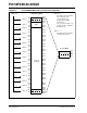
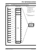
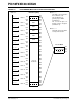
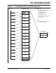
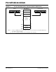
TABLE 5-2: REGISTER FILE SUMMARY (PIC18F2XK20/4XK20) (CONTINUED)
File Name Bit 7 Bit 6 Bit 5 Bit 4 Bit 3 Bit 2 Bit 1 Bit 0
Value on
POR, BOR
Details
on page:
Legend: x = unknown, u = unchanged, — = unimplemented, q = value depends on condition
Note 1: The SBOREN bit is only available when the BOREN<1:0> Configuration bits = 01; otherwise it is disabled and reads as ‘0’. See
Section 4.4 “Brown-out Reset (BOR)”.
2: These registers and/or bits are not implemented on 28-pin devices and are read as ‘0’. Reset values are shown for 40/44-pin devices;
individual unimplemented bits should be interpreted as ‘-’.
3: The PLLEN bit is only available in specific oscillator configuration; otherwise it is disabled and reads as ‘0’. See Section 2.6.2 “PLL in
HFINTOSC Modes”.
4: The RE3 bit is only available when Master Clear Reset is disabled (MCLRE Configuration bit = 0). Otherwise, RE3 reads as ‘0’. This bit is
read-only.
5: RA6/RA7 and their associated latch and direction bits are individually configured as port pins based on various primary oscillator modes.
When disabled, these bits read as ‘0’.
6: All bits of the ANSELH register initialize to ‘0’ if the PBADEN bit of CONFIG3H is ‘0’.
7: This register is only implemented in the PIC18F46K20 and PIC18F26K20 devices.